Friday, 29 March 2019

IMPROVED EXTENDED XY ON-CHIP ROUTING IN DIAMETRICAL 2D MESH NOC

IMPROVED EXTENDED XY ON-CHIP ROUTING IN DIAMETRICAL 2D MESH NOC
Prasun Ghosal and Tuhin Subhra Das
Bengal Engineering and Science University, Shibpur Howrah 711103, INDIA

ABSTRACT

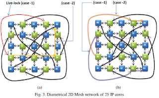
Network-on-Chip (NoC) is a new approach for designing the communication subsystem among IP cores in a System-on-Chip (SoC). NoC applies networking theory and related methods to on-chip communication and brings out notable improvements over conventional bus and crossbar interconnections. NoC offers a great improvement over the issues like scalability, productivity, power efficiency and signal integrity challenges of complex SoC design. In an NoC, the communication among different nodes is achieved by routing packets through a pre-designed network fabric according to some routing algorithm. Therefore, architecture and related routing algorithm play an important role to the improvement of overall performance of an NoC. A Diametrical 2D Mesh routing architecture has the facility of having some additional diagonal links with simple 2D Mesh architecture. In this work, we have proposed a Modified Extended 2D routing algorithm for this architecture, which will ensure that a packet always reaches the destination through the possible shortest path, and the path is always deadlock free.

KEYWORDS

NoC routing, Diametrical 2D mesh routing, On-chip communication, Extended XY routing 


Thursday, 28 March 2019

DESIGN OF A RECONFIGURABLE DSP PROCESSOR WITH BIT EFFICIENT RESIDUE NUMBER SYSTEM1

DESIGN OF A RECONFIGURABLE DSP PROCESSOR WITH BIT EFFICIENT RESIDUE NUMBER SYSTEM1
Chaitali Biswas Dutta1, Partha Garai2 and Amitabha Sinha3
1Research Scholar, Dept of CSE, University of Kalyani, India
Assistant Professor, Dept of Computer Application, Girijananda Chowdhury Institute of Management & Technology, Guwahati, India
2Machine Intelligence Unit, Indian Statistical Institute, Kolkata, 203, BT Road, Kolkata - 700108, India
3School of Information Technology, West Bengal University of Technology, BF-142, Sector-1, Salt Lake City, Kolkata-700064, India

ABSTRACT

Residue Number System (RNS), which originates from the Chinese Remainder Theorem, offers a promising future in VLSI because of its carry-free operations in addition, subtraction and multiplication. This property of RNS is very helpful to reduce the complexity of calculation in many applications. A residue number system represents a large integer using a set of smaller integers, called residues. But the area overhead, cost and speed not only depend on this word length, but also the selection of moduli, which is a very crucial step for residue system. This parameter determines bit efficiency, area, frequency etc. In this paper a new moduli set selection technique is proposed to improve bit efficiency which can be used to construct a residue system for digital signal processing environment. Subsequently, it is theoretically proved and illustrated using examples, that the proposed solution gives better results than the schemes reported in the literature. The novelty of the architecture is shown by comparison the different schemes reported in the literature. Using the novel moduli set, a guideline for a Reconfigurable Processor is presented here that can process some predefined functions. As RNS minimizes the carry propagation, the scheme can be implemented in Real Time Signal Processing & other fields where high speed computations are required. 


Wednesday, 27 March 2019

DEVICE CHARACTERISATION OF SHORT CHANNEL DEVICES AND ITS IMPACT ON CMOS CIRCUIT DESIGN

DEVICE CHARACTERISATION OF SHORT CHANNEL DEVICES AND ITS IMPACT ON CMOS CIRCUIT DESIGN
Kiran Agarwal Gupta1, Dinesh K Anvekar2 and Venkateswarlu V3
1Department of Electronics & Communication, DSCE, Visvesvaraya Technology University, Bengaluru-78 (INDIA)
2Innovations & Six Sigma Specialist, Honeywell Technology Solutions Lab, Bengaluru-560078 (INDIA)
3VTU Extension Centre, UTL Technologies Ltd., Bengaluru-560022 (INDIA).

ABSTRACT

Semiconductor technology has reached an end in the manufacture of conventional Metal Oxide semiconductor Field Effect Transistor (MOSFET). The continuous scaling of semiconductor devices has kept pace with Moore’s law and transistors below 1µm are grouped under deep sub-micron (DSM) technology node. But this trend seem to end beyond deep sub micron levels due to main design constraints such as short channel effects (SCE) , and variations in process design parameters leading to high leakage currents. Silicon material processes technology has undergone a change in process material and technology beyond 180nm node. For DSM technology nodes leakage current dominates the devices. Circuit designing using MOSFETs at deep sub micron levels, needs a careful study of the behaviour of short channel devices for the parameter variations such as threshold voltage, channel length leading to high leakage currents and poor performance of devices. In this paper we have presented the behaviour of NMOS metal oxide semiconductor field effect transistor (MOSFETs) for 90nm technology node in detail and finally compared with 180nm and 45nm nodes. The simulations have been carried out using libraries from TSMC foundry and the device has been simulated using Virtuoso Cadence Spectre Simulator version 6.1.5 with HSPICE.

KEYWORDS

MOSFETs; Technology node; process parameter variations; Short Channel Effects; DIBL; leakage current; low power; 


Monday, 25 March 2019

A High-Speed, Low Power Consumption Positive Edge Triggered D Flip-Flop for High Speed Phase Frequency Detector in 180 nm CMOS Technology

A High-Speed, Low Power Consumption Positive Edge Triggered D Flip-Flop for High Speed Phase Frequency Detector in 180 nm CMOS Technology
Prof. R .H. Talwekar, Prof. (Dr.) S.S Limaye
Deptt. Of Electronics and Telecommunication, DIMAT, Raipur.
Deptt. Of Electronics and Telecommunication, JIT, Nagpur.

ABSTRACT

A high speed low power consumption positive edge triggered Delayed (D) flip-flop was designed for increasing the speed of counter in Phase locked loop, using 180 nm CMOS technology. The designed counter has been used in the divider chip of the phase locked loop. A divide counter is required in the feedback loop to increase the VCO frequency above the input reference frequency. The proposed circuit is faster than conventional circuit as it has fast reset operation. The circuit consumes less power as it prevents short circuit power consumption. The circuit operates at 1.8V power supply. This work has been used in the design. of 2.4 GHz CMOS PLL targeting OFDM application. The CMOS based fast D-ff circuit has designed and simulated by Virtuoso tool of CADENCE spectre

KEYWORDS

Phase locked loop (PLL), Delayed flip-flop (D-ff), Phase frequency detector (PFD),True signal phase clock (TSPC), Voltage controlled oscillator (VCO), Charge pump (CP), Divider (Div), Low pass filter (LPF). 


Thursday, 21 March 2019

AN EFFICIENT APPROACH FOR FOUR-LAYER CHANNEL ROUTING IN VLSI DESIGN

AN EFFICIENT APPROACH FOR FOUR-LAYER CHANNEL ROUTING IN VLSI DESIGN
Ajoy Kumar Khan1, Bhaskar Das2 and Tapas Kumar Bayen3
1Department of Information Technology, Assam University, Silchar, India
2Department of Information Technology, Assam University, Silchar, India
3Department of Computer Science and Engineering, N. I. S. T, Berhampur, India

ABSTRACT

Channel routing is a key problem in VLSI physical design. The main goal of the channel routing problem is to reduce the area of an IC chip. If we concentrate on reducing track number in channel routing problem then automatically the area of an IC chip will be reduced. Here, we propose a new algorithm to reduce the number of tracks using four layers (two horizontal layers and two vertical layers). To be more specific, through this algorithm we convert a two-layer channel routing problem into a four-layer channel routing problem using VCG of the channel. Next, we show the experimental results and graphical structure of that solution.

KEYWORDS

Track, Channel routing, Manhattan routing model, VCG & Merging. 


Wednesday, 20 March 2019

A XOR THRESHOLD LOGIC IMPLEMENTATION THROUGH RESONANT TUNNELING DIODE

A XOR THRESHOLD LOGIC IMPLEMENTATION THROUGH RESONANT TUNNELING DIODE
Nitesh Kumar Dixit1 and Vinod Kumari2
1, 2Department of Electronics and Communication Engineering, BIET, Sikar

ABSTRACT

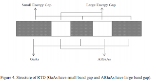
Resonant tunneling diodes (RTDs) have functional versatility and high speed switching capability. The integration of resonant tunneling diodes and MOS transistor makes threshold gates and logics. The design and fabrication of linear threshold gates will be presented based on a monostable bistable transition logic element. Each of its input terminals consist out of a resonant tunnelling diode merged with a transistor device. The circuit models of RTD and MOSFET are simulated in HSPICE. Two input XOR gate is designed and tested.

Keywords

MOSFET, RTD, SPICE, Threshold, TLG


Saturday, 16 March 2019

DESIGN & ANALYSIS OF A CHARGE RE-CYCLE BASED NOVEL LPHS ADIABATIC LOGIC CIRCUITS FOR LOW POWER APPLICATIONS

DESIGN & ANALYSIS OF A CHARGE RE-CYCLE BASED NOVEL LPHS ADIABATIC LOGIC CIRCUITS FOR LOW POWER APPLICATIONS
Sanjeev Rai1, Govind Krishna Pal2, Ram Awadh Mishra3 and Sudarshan Tiwari4
1Department of Electronics & Communication Engineering, Motilal Nehru National Institute of Technology, Allahabad, India
2Apache Design Solutions, Noida, India
3Department of Electronics & Communication Engineering, Motilal Nehru National Institute of Technology, Allahabad, India
4Director National Institute of Technology, Raipur, Chhatisgarh, India

ABSTRACT

This paper focuses on principles of adiabatic logic, its classification and comparison of various adiabatic logic designs. An attempt has been made in this paper to modify 2PASCL (Two Phase Adiabatic Static CMOS Logic) adiabatic logic circuit to minimize delay of the different 2PASCL circuit designs. This modifications in the circuits leads to improvement of Power Delay Product (PDP) which is one of the figure of merit to optimize the circuit with factors like power dissipation and delay of the circuit. This paper investigates the design approaches of low power adiabatic gates in terms of energy dissipation and uses of Simple PN diode instead of MOS diode which reduces the effect of Capacitances at high transition and power clock frequency. A computer simulation using SPECTRE from Cadence is carried out on different adiabatic circuits, such as Inverter, NAND, NOR, XOR and 2:1 MUX.

KEYWORDS

Adiabatic logic, Low-power, Two phase clocked, Energy recovery, Split-level, Diode based logic, Power Delay Product (PDP), LPHS (Low Power High Speed). 


Friday, 15 March 2019

HIGH FIN WIDTH MOSFET USING GAA STRUCTURE

HIGH FIN WIDTH MOSFET USING GAA STRUCTURE
S.L.Tripathi1, Ramanuj Mishra2, R.A.Mishra3
Department of Electronics and Communication Engineering, MNNIT, Allahabad

ABSTRACT

This paper describes the design and optimization of gate-all-around (GAA) MOSFETs structures. The optimum value of Fin width and Fin height are investigated for superior subthreshold behavior. Also the performance of Fin shaped GAA with gate oxide HfO2 are simulated and compared with conventional gate oxide SiO2 for the same structure. As a result, it was observed that the GAA with high K dielectric gate oxide has more possibility to optimize the Fin width with improved performance. All the simulations are performed on 3-D TCAD device simulator.

KEYWORDS

Gate all around(GAA),TG FinFET, High K gate oxide, Silicon-On-Insulator(SOI), Work function, Short channel effect, DIBL, Subthreshold Slope,3-D Sentaurus TCAD tool. 


Thursday, 7 March 2019

DESIGN AND IMPLEMENTATION OF ANALOG MULTIPLIER WITH IMPROVED LINEARITY 
Nandini A.S1, Sowmya Madhavan2 and Dr Chirag Sharma3
1Department of Electronics and Communication Engineering, Nitte Meenakshi Institute of Technology, Yelahanka, Bangalore- 560064
2Department of Electronics and Communication Engineering, Nitte Meenakshi Institute of Technology, Yelahanka, Bangalore- 560064
3Department of Electronics and Communication Engineering, Nitte Meenakshi Institute of Technology, Yelahanka, Bangalore- 560064

ABSTRACT

Analog multipliers are used for frequency conversion and are critical components in modern radio frequency (RF) systems. RF systems must process analog signals with a wide dynamic range at high frequencies. A mixer converts RF power at one frequency into power at another frequency to make signal processing easier and also inexpensive. A fundamental reason for frequency conversion is to allow amplification of the received signal at a frequency other than the RF, or the audio, frequency. This paper deals with two such multipliers using MOSFETs which can be used in communication systems. They were designed and implemented using 0.5 micron CMOS process. The two multipliers were characterized for power consumption, linearity, noise and harmonic distortion. The initial circuit simulated is a basic Gilbert cell whose gain is fairly high but shows more power consumption and high total harmonic distortion. Our paper aims in reducing both power consumption and total harmonic distortion. The second multiplier is a new architecture that consumes 43.07 percent less power and shows 22.69 percent less total harmonic distortion when compared to the basic Gilbert cell. The common centroid layouts of both the circuits have also been developed.

KEYWORDS

Multiplier, Gilbert cell, Noise spectral density, Total Harmonic Distortion, Transconductance 


Friday, 1 March 2019

A METHODOLOGY FOR IMPROVEMENT OF ROBA MULTIPLIER FOR ELECTRONIC APPLICATIONS
1Angila Rose Daniel and 2B. Deepa
1M.Tech in VLSI and embedded systems, Kerala technical university, India
2Assistant professor, EC Department, Kerala technical university, India

ABSTRACT

In this paper, propose an approximate multiplier that is high speed yet energy efficient. The approach is to around the operands to the closest exponent of 2. This way the machine intensive a part of the multiplication is omitted up speed and energy consumption. The potency of the planned multiplier factor is evaluated by comparing its performance with those of some approximate and correct multipliers using different design parameters. In this proposed approach combined the conventional RoBA multiplier with Kogge-stone parallel prefix adder. The results revealed that, in most (all) cases, the newly designed RoBA multiplier architectures outperformed the corresponding approximate (exact) multipliers. Thus improved the parameters of RoBA multiplier which can be used in the voice or image smoothing applications in the DSP.

KEYWORDS

Accuracy, approximate computing, efficient, error analysis, high speed multiplier, RoBa architecture, kogge stone adder, DSP processing


IMPACT OF DEVICE PARAMETERS OF TRIPLE GATE SOI-FINFET ON THE PERFORMANCE OF CMOS INVERTER AT 22NM
Prathima. A1, Kiran Bailey 2 , K.S.Gurumurthy 3
1, 2 Department of Electronics and Communication Engineering, BMSCE, Bangalore
3Department of ECE, UVCE, Bangalore University, Bangalore

ABSTRACT

A simulation based design evaluation is reported for SOI FinFETs at 22nm gate length. The impact of device parameters on the static power dissipation and delay of a CMOS inverter is presented. Fin dimensions such as Fin width and height are varied. For a given gate oxide thickness increasing the fin height and fin width degrades the SCEs, while improves the performance. It was found that reducing the fin thickness was beneficial in reducing the off state leakage current (IOFF), while reducing the fin height was beneficial in reducing the gate leakage current (IGATE). It was found that Static power dissipation of the inverter increases with fin height due to the increase in leakage current, whereas delay decreased with increase fin width due to higher on current. The performance of the inverter decreased with the downscaling of the gate oxide thickness due to higher gate leakage current and gate capacitance.

KEYWORDS

DIBL, Process and Device simulation, SCEs, SOI FinFETs, Sub threshold Slope, TCAD