Showing posts with label SRAM. Show all posts

Wednesday, 2 February 2022

Using CMOS Sub-Micron Technology VLSI Implementation of Low Power, High Speed SRAM Cell and DRAM Cell

Viplav A. Soliv and Ajay A. Gurjar, Sipna's college of Engineering & Technology, India

ABSTRACT

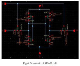
This paper deals with the design and analysis of high speed Static Random Access Memory (SRAM) cell and Dynamic Random Access Memory (DRAM) cell to develop low power consumption. SRAM and DRAM cells have been the predominant technologies used to implement memory cells in computer systems, each one having its advantages and shortcomings. SRAM cells are faster and require no refresh since reads are not destructive. In contrast, DRAM cells provide higher density and minimal leakage energy. Here we use 12-transistor SRAM cell built from a simple static latch and tri state inverter. The reading action itself refreshes the content of memory. The SRAM access path is split into two portions: from address input to word line rise (the row decoder) and from word line rise to data output (the read data path). The decoder which constitutes the path from address input to the word line rise is implemented as a binary structure by implementing a multi-stage path. The key to low power operation in the SRAM data path is to reduce the signal swings on the high capacitance nodes like the bit lines and the data lines.

KEYWORDS


SRAM, DRAM, Low power, 12-T SRAM cell

Original Source URL: https://aircconline.com/vlsics/V2N4/2411vlsics12.pdf

https://airccse.org/journal/vlsi/vol2.html


Wednesday, 6 May 2020

IMPLEMENTATION OF LOW POWER ADIABATIC SRAM

IMPLEMENTATION OF LOW POWER ADIABATIC SRAM

Savitha S M1, H P Rajani2 and Shivaling M Hunagund3
1Department of Electronics and Communication, Visvesvaraya Technological University, Belagavi, Karnataka
2HOD of Department of Telecommunication
3Asst Prof. of Department of Electronics and Communication

ABSTRACT

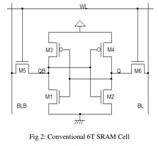
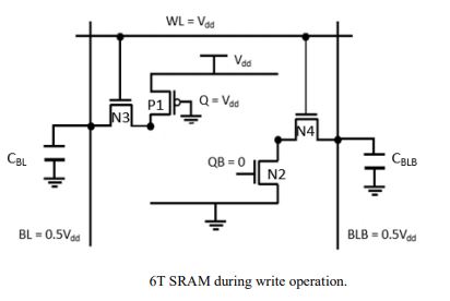
In the featuring VLSI era, compact electronic devices are popular. The reliability and durability of such compact devices relies on low power utilization. The purpose of this project was to implement a low power adiabatic Static Random Access Memory (SRAM), with the following objectives - To reduce the power waste by means of stepwise charging using tank capacitors which is an adiabatic way of generating power clock. This method is capable of recuperating the electrical energy back to the source. Further to examine the Static Noise Margin (SNM) – a parameter which gives detailed information about the cell stability – in contrast with conventional 6T, 7T and 8T topologies of SRAM under 180 nm technology. Finally, SNM variations with respect to process parameters are also discussed. All the implementations and analysis were made using CADENCE tool and MATLAB tool.

KEYWORDS

SRAM, Adiabatic, CMOS, Stepwise Charging, SNM and Process variations.