IMPLEMENTATION OF LOW POWER ADIABATIC SRAM
Savitha S M1, H P Rajani2 and Shivaling M Hunagund3
1Department of Electronics and Communication, Visvesvaraya Technological University, Belagavi, Karnataka
2HOD of Department of Telecommunication
3Asst Prof. of Department of Electronics and Communication
ABSTRACT
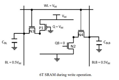
In the featuring VLSI era, compact electronic devices are popular. The reliability and durability of such compact devices relies on low power utilization. The purpose of this project was to implement a low power adiabatic Static Random Access Memory (SRAM), with the following objectives - To reduce the power waste by means of stepwise charging using tank capacitors which is an adiabatic way of generating power clock. This method is capable of recuperating the electrical energy back to the source. Further to examine the Static Noise Margin (SNM) – a parameter which gives detailed information about the cell stability – in contrast with conventional 6T, 7T and 8T topologies of SRAM under 180 nm technology. Finally, SNM variations with respect to process parameters are also discussed. All the implementations and analysis were made using CADENCE tool and MATLAB tool.
KEYWORDS
SRAM, Adiabatic, CMOS, Stepwise Charging, SNM and Process variations.
Original Source URL : https://aircconline.com/vlsics/V9N3/9318vlsi01.pdf


No comments:
Post a Comment