Showing posts with label CMOS. Show all posts

Wednesday, 11 May 2022

Power Comparison of CMOS and Adiabatic Full Adder Circuits

Y. Sunil Gavaskar Reddy and V. V. G. S. Rajendra Prasad, JNT University, India

ABSTRACT

Full adders are important components in applications such as digital signal processors (DSP) architectures and microprocessors. Apart from the basic addition adders also used in performing useful operations such as subtraction, multiplication, division, address calculation, etc. In most of these systems the adder lies in the critical path that determines the overall performance of the system. In this paper conventional complementary metal oxide semiconductor (CMOS) and adiabatic adder circuits are analyzed in terms of power and transistor count using 0.18UM technology.

KEYWORDS

Low-power, adiabatic logic, Full adder, CMOS, Pass transistor logic, Positive feed back adiabatic logic, Transmission gate logic, SERF adder

Original Source URL: https://aircconline.com/vlsics/V2N3/2311vlsics06.pdf

https://airccse.org/journal/vlsi/vol2.html


Thursday, 30 December 2021

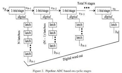
VLSI Design of Low Power High Speed 4 Bit Resolution Pipeline ADC In Submicron CMOS Technology

Ms. Rita M. Shende and Prof. Pritesh R. Gumble

Department of Electronics & Telecommunication, Sipna’s College of Engineering & Technology Amravati, Maharashtra.

Abstract

Analog-to-digital converters (ADCs) are key design blocks and are currently adopted in many application fields to improve digital systems, which achieve superior performances with respect to analog solutions. Application such as wireless communication and digital audio and video have created the need for costeffective data converters that will achieve higher speed and resolution. Widespread usage confers great importance to the design activities, which nowadays largely contributes to the production cost in integrated circuit devices (ICs). Various examples of ADC applications can be found in data acquisition systems, measurement systems and digital communication systems also imaging, instrumentation systems. Since the ADC has a continuous, infinite –valued signal as its input, the important analog points on the transfer curve x-axis for an ADC are the ones that corresponding to changes in the digital output word. These input transitions determine the amount of INL and DNL associated with the converter. Hence, we have to considered all the parameters and improving the associated performance may significantly reduce the industrial cost of an ADC manufacturing process and improved the resolution and design specially power consumption . The paper presents a design of 4 bit Pipeline ADC with low power dissipation implemented in <0.18µm.

Keyword

ADC, PIPELINE, CMOS 

Original Source URL: https://aircconline.com/vlsics/V2N4/2411vlsics08.pdf

https://airccse.org/journal/vlsi/vol2.html


Wednesday, 1 December 2021

Single bit full adder design using 8 transistors with novel 3 transistors XNOR gate

Manoj Kumar1, Sandeep K. Arya1 and Sujata Pandey2

1Department of Electronics & Communication Engineering Guru Jambheshwar University of Science & Technology, Hisar, 125 001, India

2Amity University, Noida, 201303, India

Abstract:

In present work a new XNOR gate using three transistors has been presented, which shows power dissipation of 550.7272µW in 0.35µm technology with supply voltage of 3.3V. Minimum level for high output of 2.05V and maximum level for low output of 0.084V have been obtained. A single bit full adder using eight transistors has been designed using proposed XNOR cell, which shows power dissipation of 581.542µW. Minimum level for high output of 1.97V and maximum level for low output of 0.24V is obtained for sum output signal. For carry signal maximum level for low output of 0.32V and minimum level for high output of 3.2V have been achieved. Simulations have been performed by using SPICE based on TSMC 0.35µm CMOS technology. Power consumption of proposed XNOR gate and full adder has been compared with earlier reported circuits and proposed circuit’s shows better performance in terms of power consumption and transistor count.

Keywords:

 CMOS, exclusive-OR (XOR), exclusive-NOR (XNOR), full adder, low power, pass transistor logic. 

Original Source URL: https://aircconline.com/vlsics/V2N4/2411vlsics05.pdf

https://airccse.org/journal/vlsi/vol2.html

#VLSICircuits #Testing #faulttolerence #reliability #vlsics #AIRCC


Thursday, 11 November 2021

A New Design Technique of Reversible BCD Adder Based on NMOS with Pass Transistor Gates

Md. Sazzad Hossain1, Md. Rashedul Hasan Rakib1, Md. Motiur Rahman1, A. S. M. Delowar Hossain1 and Md. Minul Hasan2

1Department of Computer Science and Engineering, Mawlana Bhashani Science & Technology University, Santosh, Tangail-1902, Bangladesh

2Amader Ltd, 5B Union Erin, 9/1 North Dhanmondi, Kalabagan, Dhaka, Bangladesh.

ABSTRACT

In this paper, we have proposed a new design technique of BCD Adder using newly constructed reversible gates are based on NMOS with pass transistor gates, where the conventional reversible gates are based on CMOS with transmission gates. We also compare the proposed reversible gates with the conventional CMOS reversible gates which show that the required number of Transistors is significantly reduced.

KEYWORDS

CMOS, Feynman gates, Fredkin gate, NMOS & pass transistor. 

Original Source URL: https://aircconline.com/vlsics/V2N4/2411vlsics02.pdf

https://airccse.org/journal/vlsi/vol2.html


Thursday, 15 April 2021

Design and Analysis of Multi Vt and Variable Vt based Pipelined Adder for Low Power applications

Shanthala S1, Cyril Prasanna Raj P2, Dr. S.Y.Kulkarni3

1Research Scholar in EC Research Centre, NMAMIT, Nitte

ABSTRACT

Majority of Digital Signal Processing (DSP) applications require arithmetic blocks such as multipliers and adders for hardware realization of complex algorithms. Power consumption of arithmetic blocks need to be minimized by use of low power techniques. In this paper, an experimental setup is developed to identify the sources of power dissipation and remedies that can be adopted to minimize power dissipation in arithmetic blocks. Use of low power techniques such as Multi Vt, variable Vt, pipelining, geometry scaling and use of appropriate load capacitance have been used to reduce power dissipation. A 4-bit pipelined adder is designed and the power dissipation is reduced to 4.17µW from 9.6µW. The designed pipelined adder can be used for DSP applications.

KEYWORD

DSP, MAC, CMOS, Pipeline, Static and Dynamic

Original Source URL: https://aircconline.com/vlsics/V1N4/1210vlsics04.pdf

http://airccse.org/journal/vlsi/vol1.html


Wednesday, 6 May 2020

IMPLEMENTATION OF LOW POWER ADIABATIC SRAM

IMPLEMENTATION OF LOW POWER ADIABATIC SRAM

Savitha S M1, H P Rajani2 and Shivaling M Hunagund3
1Department of Electronics and Communication, Visvesvaraya Technological University, Belagavi, Karnataka
2HOD of Department of Telecommunication
3Asst Prof. of Department of Electronics and Communication

ABSTRACT

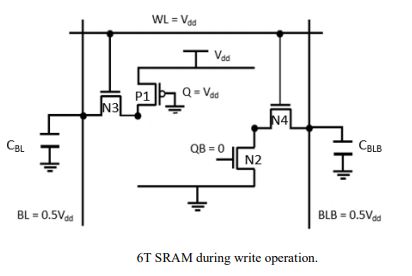
In the featuring VLSI era, compact electronic devices are popular. The reliability and durability of such compact devices relies on low power utilization. The purpose of this project was to implement a low power adiabatic Static Random Access Memory (SRAM), with the following objectives - To reduce the power waste by means of stepwise charging using tank capacitors which is an adiabatic way of generating power clock. This method is capable of recuperating the electrical energy back to the source. Further to examine the Static Noise Margin (SNM) – a parameter which gives detailed information about the cell stability – in contrast with conventional 6T, 7T and 8T topologies of SRAM under 180 nm technology. Finally, SNM variations with respect to process parameters are also discussed. All the implementations and analysis were made using CADENCE tool and MATLAB tool.

KEYWORDS

SRAM, Adiabatic, CMOS, Stepwise Charging, SNM and Process variations.