Viplav A. Soliv and Ajay A. Gurjar, Sipna's college of Engineering & Technology, India
ABSTRACT
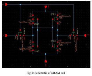
This paper deals with the design and analysis of high speed Static Random Access Memory (SRAM) cell and Dynamic Random Access Memory (DRAM) cell to develop low power consumption. SRAM and DRAM cells have been the predominant technologies used to implement memory cells in computer systems, each one having its advantages and shortcomings. SRAM cells are faster and require no refresh since reads are not destructive. In contrast, DRAM cells provide higher density and minimal leakage energy. Here we use 12-transistor SRAM cell built from a simple static latch and tri state inverter. The reading action itself refreshes the content of memory. The SRAM access path is split into two portions: from address input to word line rise (the row decoder) and from word line rise to data output (the read data path). The decoder which constitutes the path from address input to the word line rise is implemented as a binary structure by implementing a multi-stage path. The key to low power operation in the SRAM data path is to reduce the signal swings on the high capacitance nodes like the bit lines and the data lines.
KEYWORDS
SRAM, DRAM, Low power, 12-T SRAM cell
Original Source URL: https://aircconline.com/vlsics/V2N4/2411vlsics12.pdf
https://airccse.org/journal/vlsi/vol2.html


No comments:
Post a Comment