Wednesday, 26 May 2021

Low Power Reversible Parallel Binary Adder/Subtractor

Rangaraju H G1, Venugopal U2, Muralidhara K N3, Raja K B2

1Department of Telecommunication Engineering, Bangalore Institute of Technology, Bangalore, India

2Department of Electronics and Communication Engineering, University Visvesvaraya College of Engineering, Bangalore, India

3Department of Electronics and Communication Engineering, P E S College of Engineering, Mandya, Karnataka, India

Abstract

In recent years, Reversible Logic is becoming more and more prominent technology having its applications in Low Power CMOS, Quantum Computing, Nanotechnology, and Optical Computing. Reversibility plays an important role when energy efficient computations are considered. In this paper, Reversible eight-bit Parallel Binary Adder/Subtractor with Design I, Design II and Design III are proposed. In all the three design approaches, the full Adder and Subtractors are realized in a single unit as compared to only full Subtractor in the existing design. The performance analysis is verified using number reversible gates, Garbage input/outputs and Quantum Cost. It is observed that Reversible eight-bit Parallel Binary Adder/Subtractor with Design III is efficient compared to Design I, Design II and existing design.

Keywords

Reversible Logic, Garbage Input/output, Quantum Cost, Low Power, Reversible Parallel Binary Adder/Subtractor.

Original Source URL: https://aircconline.com/vlsics/V1N3/0910vlsics03.pdf

http://airccse.org/journal/vlsi/vol1.html


Wednesday, 12 May 2021

Heuristic approach to optimize the number of test cases for simple circuits

SM. Thamarai1, K.Kuppusamy2 and T. Meyyappan3

1Research scholar, 2Associate Professor&Research Supervisor, 3Associate Professor

Department of Computer Science and Engineering, Alagappa University, Karaikudi-630003, Tamilnadu, South India.

ABSTRACT

In this paper a new solution is proposed for testing simple stwo stage electronic circuits. It minimizes the number of tests to be performed to determine the genuinity of the circuit. The main idea behind the present research work is to identify the maximum number of indistinguishable faults present in the given circuit and minimize the number of test cases based on the number of faults that has been detected. Heuristic approach is used for test minimization part, which identifies the essential tests from overall test cases. From the results it is observed that, test minimization varies from 50% to 99% with the lowest one corresponding to a circuit with four gates .Test minimization is low in case of circuits with lesser input leads in gates compared to greater input leads in gates for the boolean expression with same number of symbols. Achievement of 99% reduction is due to the fact that the large number of tests find the same faults. The new approach is implemented for simple circuits. The results show potential for both smaller test sets and lower cpu times.

KEYWORDS

Adaptive Scheduled Fault Detection, CombinationalCircuits, Fault Library, Heuristic Approach , Test Minimization. 

Original Source URL: https://aircconline.com/vlsics/V1N3/0910vlsics02.pdf

http://airccse.org/journal/vlsi/vol1.html


Wednesday, 5 May 2021

A High-Swing OTA with wide Linearity for design of self-tunable linear resistor

Nikhil Raj, R.K.Sharma

Department of Electronics and Communication Engineering, National Institute of Technology, Kurukshetra Haryana, 136119, India

ABSTRACT

Low power consumption, long battery life and portability are essential requirements of modern health monitoring products. Operational Transconductance Amplifier (OTA) operating in subthreshold region is an basic building block for low power health monitoring products design. An modified design of OTA which incorporates better linearity and increased output impedance has been discussed in this paper. The proposed OTA uses High-swing improved-Wilson current mirror for low power and low-frequency applications. The achieved linearity is about ± 1.9 volt and unity gain bandwidth (UGB) of 342.30 KHz at power supply of 0.9 volt which makes OTA to consume power in range of nanowatts. The proposed low voltage OTA implementation in design of self- tunable linear resistor has been presented in this paper. The circuit implementation has been done using standard 0.18 micron technology provided by TSMC on BSIM 3v3 level-53 model parameter and verified results through use of ELDO Simulator.

KEYWORDS

Bulk-input, Wilson mirror, Linear range, MOS resistor

Original Source URL: https://aircconline.com/vlsics/V1N3/0910vlsics01.pdf

http://airccse.org/journal/vlsi/vol1.html


Thursday, 29 April 2021

Most Downloaded Article for an Year in Academia!

 International Journal of VLSI design & Communication Systems ( VLSICS ) 

ISSN: 0976 - 1357 (Online); 0976 - 1527(print)

http://airccse.org/journal/vlsi/vlsics.html

Contact Us

Here's where you can reach us: vlsicsjournal@airccse.org or vlsicsjournal@yahoo.com

Submission Deadline: May 01, 2021

Most Downloaded Article for an Year in Academia!

Verification of Driver Logic Using AMBA-AXI UVM

http://aircconline.com/vlsics/V9N3/9318vlsi03.pdf

Academia Link: https://www.academia.edu/36956674/VERIFICATION_OF_DRIVER_LOGIC_USING_AMBA_AXI_UVM


Friday, 23 April 2021

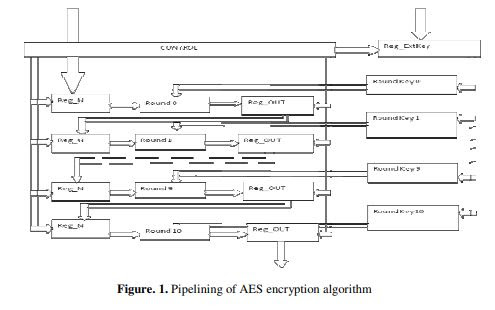
Pipelining Architecture of AES Encryption and Key Generation with Search Based Memory

Subashri T1, Arunachalam R2, Gokul Vinoth Kumar B3, Vaidehi V4

Department of Electronics, MIT Campus, Anna University, Chennai-44

Abstract.

A high speed security algorithm is always important for wired/wireless environment. The symmetric block cipher plays a major role in the bulk data encryption. One of the best existing symmetric security algorithms to provide data security is AES. AES has the advantage of being implemented in both hardware and software. Hardware implementation of the AES has the advantage of increased throughput and offers better security. Search based S-box architecture has been proposed in this paper to reduce the constraint in the hardware resources. The pipelined architecture of the AES algorithm is proposed in order to increase the throughput of the algorithm. Moreover the key schedule algorithm of the AES encryption is pipelined to get the speedup.

Keywords

AES pipelining, Key pipelining, Search Based Memory, VLSI.

Original Source URL: https://aircconline.com/vlsics/V1N4/1210vlsics05.pdf

http://airccse.org/journal/vlsi/vol1.html


Sunday, 18 April 2021

Call for Papers - International Journal of VLSI design & Communication Systems ( VLSICS )

 ISSN: 0976 - 1357 (Online); 0976 - 1527(print)


http://airccse.org/journal/vlsi/vlsics.html


Scope & Topics


International journal of VLSI design & Communication Systems (VLSICS) is a bi monthly open access peer-reviewed journal that publishes articles which contribute new results in all areas of VLSI Design & Communications. The goal of this journal is to bring together researchers and practitioners from academia and industry to focus on advanced VLSI Design & communication concepts and establishing new collaborations in these areas. 


Authors are solicited to contribute to this journal by submitting articles that illustrate research results, projects, surveying works and industrial experiences that describe significant advances in the VLSI design & Communications.


Topics of interest include, but are not limited to, the following: 


* Design

* VLSI Circuits

* Computer-Aided Design (CAD)

* Low Power and Power Aware Design

* Testing, Reliability, Fault-Tolerance

* Emerging Technologies

* Post-CMOS VLSI

* VLSI Applications (Communications, Video, Security, Sensor Networks, etc)

* Nano Electronics, Molecular, Biological and Quantum Computing

* Intellectual Property Creating and Sharing

* Wireless Communications


Paper Submission 


Authors are invited to submit papers for this journal through E-Mail: vlsicsjournal@airccse.org or through Submission System. Submissions must be original and should not have been published previously or be under consideration for publication while being evaluated for this Journal.


Important Dates:

·         Submission Deadline : April 24, 2021

·         Notification                   : May 24, 2021

·         Final Manuscript Due : May 31, 2021

·         Publication Date          : Determined by the Editor-in-Chief

Contact Us 

Here's where you can reach us : vlsicsjournal@airccse.org or vlsicsjournal@yahoo.com 

Here you can reach us in social Medias

Facebook:   https://www.facebook.com/vlsics.journal

Twitter :      https://twitter.com/vlsicsjournala1

Academia:   https://independent.academia.edu/VJournal

Google scholar Link: https://scholar.google.co.in/citations?user=ZdE-aVMAAAAJ


Thursday, 15 April 2021

Design and Analysis of Multi Vt and Variable Vt based Pipelined Adder for Low Power applications

Shanthala S1, Cyril Prasanna Raj P2, Dr. S.Y.Kulkarni3

1Research Scholar in EC Research Centre, NMAMIT, Nitte

ABSTRACT

Majority of Digital Signal Processing (DSP) applications require arithmetic blocks such as multipliers and adders for hardware realization of complex algorithms. Power consumption of arithmetic blocks need to be minimized by use of low power techniques. In this paper, an experimental setup is developed to identify the sources of power dissipation and remedies that can be adopted to minimize power dissipation in arithmetic blocks. Use of low power techniques such as Multi Vt, variable Vt, pipelining, geometry scaling and use of appropriate load capacitance have been used to reduce power dissipation. A 4-bit pipelined adder is designed and the power dissipation is reduced to 4.17µW from 9.6µW. The designed pipelined adder can be used for DSP applications.

KEYWORD

DSP, MAC, CMOS, Pipeline, Static and Dynamic

Original Source URL: https://aircconline.com/vlsics/V1N4/1210vlsics04.pdf

http://airccse.org/journal/vlsi/vol1.html