Wednesday, 28 July 2021

Efficient Hardware Co-Simulation of Down Convertor for Wireless Communication Systems

Rajesh Mehra and Swapna Devi

Department of Electronics & Communication Engineering, Sector-26, NITTTR, Chandigarh, UT, India 

ABSTRACT

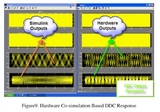
In this paper an optimized hardware co-simulation approach is presented to design & implement GSM based digital down convertor for Software Defined Radios. The proposed DDC is implemented using optimal equiripple technique to reduce the resource requirement. A computationally efficient polyphase decomposition structure is used to improve the hardware complexity of the overall design. The proposed model is implemented by using embedded multipliers, LUTs and BRAMs of target device to enhance the system performance in terms of speed and area. The DDC model is designed and simulated with Simulink and Xilinx System Generator, synthesized with Xilinx Synthesis Tool (XST) and implemented on Virtex-II Pro based xc2vp30-7ff896 FPGA device. The results show that proposed design can operate at maximum frequency of 160 MHz by consuming power of 0.34004W 25 °C junction temperature. The proposed design is consuming very less resources available on target device to provide cost effective solution for SDR based wireless applications.

KEYWORDS

ASIC, BRAM, FPGA, GSM, LUT & SDR 

Original Source URL: https://aircconline.com/vlsics/V1N2/0610vlsics2.pdf

https://airccse.org/journal/vlsi/vol1.html


Thursday, 15 July 2021

Design of Low Power Phase Locked Loop (PLL) Using 45NM VLSI Technology

Ms. Ujwala A. Belorkar 1 and Dr. S.A.Ladhake2

1Department of electronics & telecommunication ,Hanuman Vyayam Prasarak Mandal’s College of Engineering & Technology, Amravati. Maharashtra.

2Sipana’s College of Engineering & Technology, Amravati, Maharashtra.

ABSTRACT

 Power has become one of the most important paradigms of design convergence for multi gigahertz communication systems such as optical data links, wireless products, microprocessor & ASIC/SOC designs. POWER consumption has become a bottleneck in microprocessor design. The core of a microprocessor, which includes the largest power density on the microprocessor. In an effort to reduce the power consumption of the circuit, the supply voltage can be reduced leading to reduction of dynamic and static power consumption. Lowering the supply voltage, however, also reduces the performance of the circuit, which is usually unacceptable. One way to overcome this limitation, available in some application domains, is to replicate the circuit block whose supply voltage is being reduced in order to maintain the same throughput .This paper introduces a design aspects for low power phase locked loop using VLSI technology. This phase locked loop is designed using latest  45nm process technology parameters, which in turn offers high speed performance at low power. The main novelty related to the 45nm technology such as the high-k gate oxide ,metal-gate and very low-k interconnect dielectric described. VLSI Technology includes process design, trends, chip fabrication, real circuit parameters, circuit design, electrical characteristics, configuration building blocks, switching circuitry, translation onto silicon, CAD, practical experience in layout design

KEYWORDS

Phase locked loop (PLL), voltage-controlled oscillator (VCO), 45nm technology, VLSI technology, low power. 

Original Source URL: https://aircconline.com/vlsics/V1N2/0610vlsics1.pdf

https://airccse.org/journal/vlsi/vol1.html


Friday, 2 July 2021

Design of a High Precision, Wide Ranged Analog Clock Generator with Field Programmability Using Floating-Gate Transistors

Garima Kapur, C.M Markan and V. Prem Pyara, Dayalbagh Educational Institute, India

ABSTRACT

This paper presents a circuit of a high-precision, wide ranged, analog clock generator with on-chip programmability feature using Floating-gate transistors. The programmable oscillator can attain a continuous range of time-periods lying in the programming precision range of Floating Gates. The circuit consists of two sub circuits: Current Generator circuit and Wave Generator circuit. The current of current generator circuit is programmable and mirrored to the wave generator to generate the desired square wave. The topology is well suited to applications like clocking high performance ADCs and DACs as well as used as the internal clock in structured analog CMOS designs. A simulation model of the circuit was built in T-Spice, 0.35µm CMOS process. The circuit results in finely tuned clock with programmability precision of about 13bit [1]. Simulation results show high amount of temperature insensitivity (0.507ns/°C) for a large range of thermal conditions. The proposed circuit can compensate any change in temperature. The circuit design can be operated at low supply voltage i.e., 1v.

KEYWORDS

Square wave generator, floating gate FET, field programmability

Original Source URL: https://aircconline.com/vlsics/V1N3/0910vlsics05.pdf

http://airccse.org/journal/vlsi/vol1.html


Tuesday, 15 June 2021

8th International Conference on Signal, Image Processing and Multimedia (SPM 2021)

 September 25 ~ 26, 2021, Toronto, Canada

https://cseit2021.org/spm/index

SCOPE

8th International Conference on Signal, Image Processing and Multimedia (SPM 2021) is a forum for presenting new advances and research results in the fields of Signal, Image Processing and Multimedia. The conference will bring together leading researchers, engineers and scientists in the domain of interest from around the world. Authors are solicited to contribute to the conference by submitting articles that illustrate research results, projects, surveying works and industrial experiences.


Authors are solicited to contribute to the conference by submitting articles that illustrate research results, projects, surveying works and industrial experiences that describe significant advances in the following areas, but are not limited to.

TO PI CS OF IN TE RES T

·         Human Biometrics and Security Systems

·         Internet of Things Technology

·         Medical Signal Acquisition, Analysis and Processing

·         Multimedia Security and Forensics

·         Signal and Information Processing for Smart Systems

·         Applied Digital Signal Processing

·         Audio, Image, Video processing

·         Biomedical Signal Processing and System

·         Coding and Transmission

·         Computer Graphics and Visualization

·         Computer Vision

·         Data Analytics and Machine Learning

·         Deep Learning: Algorithms, Implementations, and applications

·         Digital Multimedia Broadcasting

·         Digital Signal Processing in Communications

·         Education and Training

·         Emerging Technologies in Digital Signal Processing

·         Emerging Technologies

·         Image & Signal Processing Applications

·         Image Acquisition and Display

·         Image and Video Processing & Analysis

·         Image Formation

·         Image Scanning, Display, and Printing

·         Machine learning, Computer Graphics, Biological Vision

·         Multimedia analysis and Internet

·         Multimedia and Artificial Intelligence

·         Multimedia Applications

·         Multimedia Communication and Networking

·         Multimedia Content Understanding

·         Multimedia Databases and File Systems

·         Multimedia Human-Machine Interface and Interaction

·         Multimedia Interface and Interaction

·         Multimedia Security and Content Protection

·         Multimedia Signal Processing

·         Multimedia Standards and Related Issues

·         Multimedia Systems and Devices

·         Multimedia

·         Operating System Mechanisms for Multimedia

·         Signal and Image Processing

·         Signal and Information Processing in Education

·         Storage and Retrieval

·         Virtual Reality and 3-D Imaging

·         Wireless, Mobile Computing and Multimedia

PAPER SUBMISSION

Authors are invited to submit papers through the conference Submission System by June 19, 2021. Submissions must be original and should not have been published previously or be under consideration for publication while being evaluated for this conference. The proceedings of the conference will be published by Computer Science Conference Proceedings in Computer Science & Information Technology (CS & IT) series (Confirmed).


Selected papers from SPM 2021, after further revisions, will be published in the special issue of the following journals


·         Signal & Image Processing : An International Journal (SIPIJ)

·         International Journal of VLSI Design & Communication Systems (VLSICS)

·         International Journal of Multimedia & Its Applications (IJMA)

·         International Journal of Embedded Systems and Applications (IJESA)

·         Information Technology in Industry (ITII)New - ESCI-Thomson Reuters Indexed

IMPORTANT DATES

·         Submission Deadline: June 19, 2021

·         Authors Notification: July 20, 2021

·         Registration & Camera-Ready Paper Due : July 28, 2021

CONTACT US

Here's where you can reach us: spm@cseit2021.org or spmconf@yahoo.com

SUBMISSION SYSTEM

https://cseit2021.org/submission/index.php


Tuesday, 8 June 2021

Statistical Modelling of ft to Process Parameters in 30 NM Gate Length Finfets

B. Lakshmi and R. Srinivasan

Department of Information Technology, SSN College of Engineering, Kalavakkam – 603 110, Chennai, India

ABSTRACT

This paper investigates the effect of process variations on unity gain frequency (ft) in 30 nm gate length FinFET by performing extensive TCAD simulations. Six different geometrical parameters, channel doping, source/drain doping and gate electrode work function are studied for their sensitivity on ft . It is found that ft  is more sensitive to gate length, underlap, gate-oxide thickness, channel and Source/Drain doping and less sensitive to source/drain width and length, and work function variations. Statistical modelling has been performed for ft  through design of experiment with respect to sensitive parameters. The model has been validated through a comparison between random set of experimental data simulations and predicted values obtained from the model.

KEYWORDS

ft , FinFET, process variations, Statistical modelling, Design of Experiments

Original Source URL: https://aircconline.com/vlsics/V1N3/0910vlsics04.pdf

http://airccse.org/journal/vlsi/vol1.html


Wednesday, 26 May 2021

Low Power Reversible Parallel Binary Adder/Subtractor

Rangaraju H G1, Venugopal U2, Muralidhara K N3, Raja K B2

1Department of Telecommunication Engineering, Bangalore Institute of Technology, Bangalore, India

2Department of Electronics and Communication Engineering, University Visvesvaraya College of Engineering, Bangalore, India

3Department of Electronics and Communication Engineering, P E S College of Engineering, Mandya, Karnataka, India

Abstract

In recent years, Reversible Logic is becoming more and more prominent technology having its applications in Low Power CMOS, Quantum Computing, Nanotechnology, and Optical Computing. Reversibility plays an important role when energy efficient computations are considered. In this paper, Reversible eight-bit Parallel Binary Adder/Subtractor with Design I, Design II and Design III are proposed. In all the three design approaches, the full Adder and Subtractors are realized in a single unit as compared to only full Subtractor in the existing design. The performance analysis is verified using number reversible gates, Garbage input/outputs and Quantum Cost. It is observed that Reversible eight-bit Parallel Binary Adder/Subtractor with Design III is efficient compared to Design I, Design II and existing design.

Keywords

Reversible Logic, Garbage Input/output, Quantum Cost, Low Power, Reversible Parallel Binary Adder/Subtractor.

Original Source URL: https://aircconline.com/vlsics/V1N3/0910vlsics03.pdf

http://airccse.org/journal/vlsi/vol1.html