Rajesh Mehra and Swapna Devi
Department of Electronics & Communication Engineering, Sector-26, NITTTR, Chandigarh, UT, India
ABSTRACT
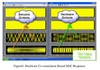
In this paper an optimized hardware co-simulation approach is presented to design & implement GSM based digital down convertor for Software Defined Radios. The proposed DDC is implemented using optimal equiripple technique to reduce the resource requirement. A computationally efficient polyphase decomposition structure is used to improve the hardware complexity of the overall design. The proposed model is implemented by using embedded multipliers, LUTs and BRAMs of target device to enhance the system performance in terms of speed and area. The DDC model is designed and simulated with Simulink and Xilinx System Generator, synthesized with Xilinx Synthesis Tool (XST) and implemented on Virtex-II Pro based xc2vp30-7ff896 FPGA device. The results show that proposed design can operate at maximum frequency of 160 MHz by consuming power of 0.34004W 25 °C junction temperature. The proposed design is consuming very less resources available on target device to provide cost effective solution for SDR based wireless applications.
KEYWORDS
ASIC, BRAM, FPGA, GSM, LUT & SDR
Original Source URL: https://aircconline.com/vlsics/V1N2/0610vlsics2.pdf
https://airccse.org/journal/vlsi/vol1.html


No comments:
Post a Comment