Thursday, 24 February 2022

International Journal of VLSI design & Communication Systems (VLSICS), H index - Profile

 International Journal of VLSI design & Communication Systems (VLSICS)

ISSN: 0976 - 1357 (Online); 0976 - 1527(print)

https://airccse.org/journal/vlsi/vlsics.html

Submission Deadline : February 04, 2023

Contact Us

Here's where you can reach us : vlsicsjournal@airccse.org or vlsics@aircconline.com or vlsicsjournal@yahoo.com

Submission System: http://coneco2009.com/submissions/imagination/home.html

International Journal of VLSI design & Communication Systems (VLSICS), H index - Profile

https://www.academia.edu/72390024/International_Journal_of_VLSI_design_and_Communication_Systems_VLSICS_H_index_Profile

Academia URL: https://independent.academia.edu/VJournal/

#VLSI #Communication #AIRCC #VLSICS #Research


Thursday, 10 February 2022

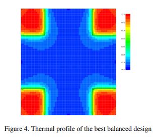
A Novel Methodology for Thermal Aware Silicon Area Estimation for 2D & 3D MPSoCs

Ramya Menon C. and Vinod Pangracious

Department of Electronics & Communication Engineering, Rajagiri School of Engineering & Technology, Kochi, Kerala 

ABSTRACT

In a multiprocessor system on chip (MPSoC) IC the processor is one of the highest heat dissipating devices. The temperature generated in an IC may vary with floor plan of the chip. This paper proposes an integration and thermal analysis methodology to extract the peak temperature and temperature distribution of 2-dimensional and 3-dimensional multiprocessor system-on-chip. As we know the peak temperature of chip increases in 3-dimensional structures compared to 2-dimensional ones due to the reduced space in intra-layer and inter-layer components. In sub-nanometre scale technologies, it is inevitable to analysis the heat developed in individual chip to extract the temperature distribution of the entire chip. With the technology scaling in new generation ICs more and more components are integrated to a smaller area. Along with the other parameters threshold voltage is also scaled down which results in exponential increase in leakage current. This has resulted in rise in hotspot temperature value due to increase in leakage power. In this paper, we have analysed the temperature developed in an IC with four identical processors at 2.4 GHz in different floorplans. The analysis has been done for both 2D and 3D arrangements. In the 3D arrangement, a three layered structure has been considered with two Silicon layers and a thermal interface material (TIM) in between them. Based on experimental results the paper proposes a methodology to reduce the peak temperature developed in 2D and 3D integrated circuits.

KEYWORDS

Hotspot, Peak Temperature, Three Dimensional Integration, Through silicon Via. 

Original Source URL: https://aircconline.com/vlsics/V2N4/2411vlsics13.pdf

https://airccse.org/journal/vlsi/vol2.html


Wednesday, 2 February 2022

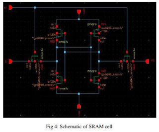
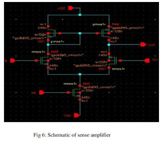
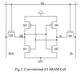
Using CMOS Sub-Micron Technology VLSI Implementation of Low Power, High Speed SRAM Cell and DRAM Cell

Viplav A. Soliv and Ajay A. Gurjar, Sipna's college of Engineering & Technology, India

ABSTRACT

This paper deals with the design and analysis of high speed Static Random Access Memory (SRAM) cell and Dynamic Random Access Memory (DRAM) cell to develop low power consumption. SRAM and DRAM cells have been the predominant technologies used to implement memory cells in computer systems, each one having its advantages and shortcomings. SRAM cells are faster and require no refresh since reads are not destructive. In contrast, DRAM cells provide higher density and minimal leakage energy. Here we use 12-transistor SRAM cell built from a simple static latch and tri state inverter. The reading action itself refreshes the content of memory. The SRAM access path is split into two portions: from address input to word line rise (the row decoder) and from word line rise to data output (the read data path). The decoder which constitutes the path from address input to the word line rise is implemented as a binary structure by implementing a multi-stage path. The key to low power operation in the SRAM data path is to reduce the signal swings on the high capacitance nodes like the bit lines and the data lines.

KEYWORDS


SRAM, DRAM, Low power, 12-T SRAM cell

Original Source URL: https://aircconline.com/vlsics/V2N4/2411vlsics12.pdf

https://airccse.org/journal/vlsi/vol2.html


Thursday, 27 January 2022

Low Power Low Voltage Bulk Driven Balanced OTA

Neha Gupta, Sapna Singh, Meenakshi Suthar and Priyanka Soni

Faculty of Engineering Technology, Mody Institute of Technology and Science, Lakshmangarh, Sikar, India

ABSTRACT

The last few decades, a great deal of attention has been paid to low-voltage (LV) low-power (LP) integrated circuits design since the power consumption has become a critical issue. Among many techniques used for the design of LV LP analog circuits, the Bulk-driven principle offers a promising route towards this design for many aspects mainly the simplicity and using the conventional MOS technology to implement these designs. This paper is devoted to the Bulk-driven (BD) principle and utilizing this principle to design LV LP building block of Operational Transconductance Amplifier (OTA) in standard CMOS processes and supply voltage 0.9V. The simulation results have been carried out by the Spice simulator using the 130nm CMOS technology from TSMC.

KEYWORDS

Bulk-driven MOS, OTA, BOTA, Body effect

Original Source URL: https://aircconline.com/vlsics/V2N4/2411vlsics11.pdf

https://airccse.org/journal/vlsi/vol2.html


Thursday, 20 January 2022

Design and ASIC Implemenatation of DUC/DDC for Communication Systems

Naagesh S. Bhat

Senior Product Engineer, Green Mil International Ltd., Bangalore, India

ABSTRACT

Communication systems use the concept of transmitting information using the electrical distribution network as a communication channel. To enable the transmission data signal modulated on a carrier signal is superimposed on the electrical wires. Typical power lines are designed to handle 50/60 Hz of AC power signal; however they can carry the signals up to 500 KHz frequency. This work aims to aid transmission/reception of an audio signal in the spectrum from 300 Hz to 4000 Hz using PLCC on a tunable carrier frequency in the spectrum from 200 KHz to 500 KHz. For digital amplitude modulation the sampling rate of the carrier and the audio signal has to be matched. Tunable carrier generation can be achieved with Direct Digital Synthesizers at a desired sampling rate. DSP Sample rate conversion techniques are very useful to make the sampling circuits to work on their own sampling rates which are fine for the data/modulated-carrier signal’s bandwidth. This also simplifies the complexity of the sampling circuits. Digital Up Conversion (DUC) and Digital Down Conversion (DDC) are DSP sample rate conversion techniques which refer to increasing and decreasing the sampling rate of a signal respectively. 

The objective was to design and implement low power ASIC of DUC and DDC designs at 65nm for PLCC. Low power implementation was carried out using Multi-VDD technique. MATLAB software models were used to understand the DUC and DDC designs. RTL to GDS flow was executed using Synopsys tools such as VCS, Design Compiler, IC Compiler and PrimeTime. Key milestones of this activity are RTL verification, synthesis, gate-level simulations, low power architecture definitions, physical implementation, ASIC signoff checks and postroute delay based simulations. Multi-VDD technique deployed on DUC and DDC helped to reduce the power consumption from 280.9uW to 198.07uW and from 176.26uW to 124.47uW respectively. DUC and DUC designs have met functionality at 64MHz clock frequency. Both the designs have passed postroute delay based simulations, static performance checks, power domain checks and TSMC’s 65nm design rule checks.

KEYWORDS

Power Line Carrier Communication, Digital Down-Counter, Digital Up-Counter, Application Specific Integrated Circuit, Multi-VDD, TSMC 

Original Source URL: https://aircconline.com/vlsics/V2N4/2411vlsics10.pdf

https://airccse.org/journal/vlsi/vol2.html


Thursday, 13 January 2022

An Efficient FPGA Implemenation of MRI Image Filtering and Tumour Characterization Using XILINX System Generator

S. Allin Christe, M. Vignesh and A. Kandaswamy, PSG College of Technology, India

ABSTRACT

This paper presents an efficient architecture for various image filtering algorithms and tumor characterization using Xilinx System Generator (XSG). This architecture offers an alternative through a graphical user interface that combines MATLAB, Simulink and XSG and explores important aspects concerned to hardware implementation. Performance of this architecture implemented in SPARTAN-3E Starter kit (XC3S500E-FG320) exceeds those of similar or greater resources architectures. The proposed architecture reduces the resources available on target device by 50%.

KEYWORDS

MRI, Matlab, Xilinx System Generator, FPGA, Edge Detection

Original Source URL: https://aircconline.com/vlsics/V2N4/2411vlsics09.pdf

https://airccse.org/journal/vlsi/vol2.html


Thursday, 6 January 2022