Thursday 24 February 2022

International Journal of VLSI design & Communication Systems (VLSICS), H index - Profile

 International Journal of VLSI design & Communication Systems (VLSICS)

ISSN: 0976 - 1357 (Online); 0976 - 1527(print)

https://airccse.org/journal/vlsi/vlsics.html

Submission Deadline : February 04, 2023

Contact Us

Here's where you can reach us : vlsicsjournal@airccse.org or vlsics@aircconline.com or vlsicsjournal@yahoo.com

Submission System: http://coneco2009.com/submissions/imagination/home.html

International Journal of VLSI design & Communication Systems (VLSICS), H index - Profile

https://www.academia.edu/72390024/International_Journal_of_VLSI_design_and_Communication_Systems_VLSICS_H_index_Profile

Academia URL: https://independent.academia.edu/VJournal/

#VLSI #Communication #AIRCC #VLSICS #Research


Thursday 10 February 2022

A Novel Methodology for Thermal Aware Silicon Area Estimation for 2D & 3D MPSoCs

Ramya Menon C. and Vinod Pangracious

Department of Electronics & Communication Engineering, Rajagiri School of Engineering & Technology, Kochi, Kerala 

ABSTRACT

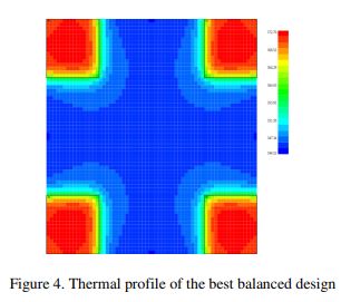
In a multiprocessor system on chip (MPSoC) IC the processor is one of the highest heat dissipating devices. The temperature generated in an IC may vary with floor plan of the chip. This paper proposes an integration and thermal analysis methodology to extract the peak temperature and temperature distribution of 2-dimensional and 3-dimensional multiprocessor system-on-chip. As we know the peak temperature of chip increases in 3-dimensional structures compared to 2-dimensional ones due to the reduced space in intra-layer and inter-layer components. In sub-nanometre scale technologies, it is inevitable to analysis the heat developed in individual chip to extract the temperature distribution of the entire chip. With the technology scaling in new generation ICs more and more components are integrated to a smaller area. Along with the other parameters threshold voltage is also scaled down which results in exponential increase in leakage current. This has resulted in rise in hotspot temperature value due to increase in leakage power. In this paper, we have analysed the temperature developed in an IC with four identical processors at 2.4 GHz in different floorplans. The analysis has been done for both 2D and 3D arrangements. In the 3D arrangement, a three layered structure has been considered with two Silicon layers and a thermal interface material (TIM) in between them. Based on experimental results the paper proposes a methodology to reduce the peak temperature developed in 2D and 3D integrated circuits.

KEYWORDS

Hotspot, Peak Temperature, Three Dimensional Integration, Through silicon Via. 

Original Source URL: https://aircconline.com/vlsics/V2N4/2411vlsics13.pdf

https://airccse.org/journal/vlsi/vol2.html


Wednesday 2 February 2022

Using CMOS Sub-Micron Technology VLSI Implementation of Low Power, High Speed SRAM Cell and DRAM Cell

Viplav A. Soliv and Ajay A. Gurjar, Sipna's college of Engineering & Technology, India

ABSTRACT

This paper deals with the design and analysis of high speed Static Random Access Memory (SRAM) cell and Dynamic Random Access Memory (DRAM) cell to develop low power consumption. SRAM and DRAM cells have been the predominant technologies used to implement memory cells in computer systems, each one having its advantages and shortcomings. SRAM cells are faster and require no refresh since reads are not destructive. In contrast, DRAM cells provide higher density and minimal leakage energy. Here we use 12-transistor SRAM cell built from a simple static latch and tri state inverter. The reading action itself refreshes the content of memory. The SRAM access path is split into two portions: from address input to word line rise (the row decoder) and from word line rise to data output (the read data path). The decoder which constitutes the path from address input to the word line rise is implemented as a binary structure by implementing a multi-stage path. The key to low power operation in the SRAM data path is to reduce the signal swings on the high capacitance nodes like the bit lines and the data lines.

KEYWORDS


SRAM, DRAM, Low power, 12-T SRAM cell

Original Source URL: https://aircconline.com/vlsics/V2N4/2411vlsics12.pdf

https://airccse.org/journal/vlsi/vol2.html