Thursday 30 December 2021

VLSI Design of Low Power High Speed 4 Bit Resolution Pipeline ADC In Submicron CMOS Technology

Ms. Rita M. Shende and Prof. Pritesh R. Gumble

Department of Electronics & Telecommunication, Sipna’s College of Engineering & Technology Amravati, Maharashtra.

Abstract

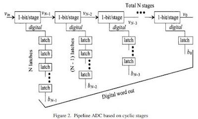
Analog-to-digital converters (ADCs) are key design blocks and are currently adopted in many application fields to improve digital systems, which achieve superior performances with respect to analog solutions. Application such as wireless communication and digital audio and video have created the need for costeffective data converters that will achieve higher speed and resolution. Widespread usage confers great importance to the design activities, which nowadays largely contributes to the production cost in integrated circuit devices (ICs). Various examples of ADC applications can be found in data acquisition systems, measurement systems and digital communication systems also imaging, instrumentation systems. Since the ADC has a continuous, infinite –valued signal as its input, the important analog points on the transfer curve x-axis for an ADC are the ones that corresponding to changes in the digital output word. These input transitions determine the amount of INL and DNL associated with the converter. Hence, we have to considered all the parameters and improving the associated performance may significantly reduce the industrial cost of an ADC manufacturing process and improved the resolution and design specially power consumption . The paper presents a design of 4 bit Pipeline ADC with low power dissipation implemented in <0.18µm.

Keyword

ADC, PIPELINE, CMOS 

Original Source URL: https://aircconline.com/vlsics/V2N4/2411vlsics08.pdf

https://airccse.org/journal/vlsi/vol2.html


Wednesday 22 December 2021

A Novel Approach to Minimize Spare Cell Leakage Power Consumption During Physical Design Implementation

Vasantha Kumar B.V.P1, Dr. N. S. Murthy Sharma2, Dr. K. Lal Kishore3 and 4Jibanjeet Mishra

1Synopsys (India) Pvt. Ltd, Hyderabad, India.

2Principal, SV Institute of Engineering and Technology, Hyderabad, India.

3JNT University, ECE Dept, Hyderabad

4Synopsys (India) Pvt. Ltd, Hyderabad, India.

ABSTRACT

In IC designs leakage power constitutes significant amount power dissipation because CMOS gates are not perfect switches. The leakage power in CMOS gates is dependent on the states of the inputs. This leakage power will get dissipated even when the gates are in idle conditions. Traditionally ECO cells (or) spare cells remain idle in the design and thus contributes to significant state dependent leakage power consumption. In this paper we proposed novel solution to minimize the state dependent leakage power dissipation of the spare cells.

KEYWORDS

Engineering Change Order (ECO), ECO cell, Spare cell, State dependent, leakage power and switching probability.

Original Source URL: https://aircconline.com/vlsics/V2N4/2411vlsics07.pdf

https://airccse.org/journal/vlsi/vol2.html


Tuesday 21 December 2021

Call for Research Papers! December Issue!

International Journal of VLSI design & Communication Systems (VLSICS)

ISSN: 0976 - 1357 (Online); 0976 - 1527(print)

http://airccse.org/journal/vlsi/vlsics.html

Contact Us

Here's where you can reach us : vlsicsjournal@airccse.org or vlsics@aircconline.com or vlsicsjournal@yahoo.com

Submission Deadline : December 25, 2021

Submission System: http://coneco2009.com/submissions/imagination/home.html

#communication #wireless #digitalcommunication #mobility #opticalcommunications


Wednesday 8 December 2021

Fault Modeling of Combinational and Sequential Circuits at Register Transfer Level

M.S.Suma1 and K.S.Gurumurthy2

1Department of Electronics and Communication Engineering, R.V.College of Engineering, Bangalore, India

2Department of Electronics and Communication Engineering, U.V.College of Engineering, Bangalore, India

ABSTRACT

 As the complexity of Very Large Scale Integration (VLSI) is growing, testing becomes tedious and tougher. As of now fault models are used to test digital circuits at the gate level or below that level. By using fault models at the lower levels, testing becomes cumbersome and will lead to delays in the design cycle. In addition, developments in deep submicron technology provide an opening to new defects. We must develop efficient fault detection and location methods in order to reduce manufacturing costs and time to market. Thus there is a need to look for a new approach of testing the circuits at higher levels to speed up the design cycle. This paper proposes on Register Transfer Level (RTL) modeling for digital circuits and computing the fault coverage. The result obtained through this work establishes that the fault coverage with the RTL fault model is comparable to the gate level fault coverage.

KEYWORDS

Automatic test pattern generation (ATPG), fault coverage, fault simulation, stuck-at fault, RTL. 

Original Source URL: https://aircconline.com/vlsics/V2N4/2411vlsics06.pdf

https://airccse.org/journal/vlsi/vol2.html


Wednesday 1 December 2021

Single bit full adder design using 8 transistors with novel 3 transistors XNOR gate

Manoj Kumar1, Sandeep K. Arya1 and Sujata Pandey2

1Department of Electronics & Communication Engineering Guru Jambheshwar University of Science & Technology, Hisar, 125 001, India

2Amity University, Noida, 201303, India

Abstract:

In present work a new XNOR gate using three transistors has been presented, which shows power dissipation of 550.7272µW in 0.35µm technology with supply voltage of 3.3V. Minimum level for high output of 2.05V and maximum level for low output of 0.084V have been obtained. A single bit full adder using eight transistors has been designed using proposed XNOR cell, which shows power dissipation of 581.542µW. Minimum level for high output of 1.97V and maximum level for low output of 0.24V is obtained for sum output signal. For carry signal maximum level for low output of 0.32V and minimum level for high output of 3.2V have been achieved. Simulations have been performed by using SPICE based on TSMC 0.35µm CMOS technology. Power consumption of proposed XNOR gate and full adder has been compared with earlier reported circuits and proposed circuit’s shows better performance in terms of power consumption and transistor count.

Keywords:

 CMOS, exclusive-OR (XOR), exclusive-NOR (XNOR), full adder, low power, pass transistor logic. 

Original Source URL: https://aircconline.com/vlsics/V2N4/2411vlsics05.pdf

https://airccse.org/journal/vlsi/vol2.html

#VLSICircuits #Testing #faulttolerence #reliability #vlsics #AIRCC