Wednesday 30 December 2020

Efficient Absolute Difference Circuit for SAD Computation On FPGA

Jaya Koshta, Kavita Khare and M.K Gupta

Maulana Azad National Institute of Technology, Bhopal

ABSTRACT

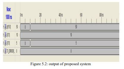
Video Compression is very essential to meet the technological demands such as low power, less memory and fast transfer rate for different range of devices and for various multimedia applications. Video compression is primarily achieved by Motion Estimation (ME) process in any video encoder which contributes to significant compression gain.Sum of Absolute Difference (SAD) is used as distortion metric in ME process.In this paper, efficient Absolute Difference(AD)circuit is proposed which uses Brent Kung Adder(BKA) and a comparator based on modified 1’s complement principle and conditional sum adder scheme. Results shows that proposed architecture reduces delay by 15% and number of slice LUTs by 42% as compared to conventional architecture. Simulation and synthesis are done on Xilinx ISE 14.2 using Virtex 7 FPGA.

KEYWORDS

HEVC, motion estimation, sum of absolute difference, parallel prefix adders, Brent Kung Adder.

ORIGINAL SOURCE URL: https://aircconline.com/vlsics/V10N2/10219vlsi01.pdf

http://airccse.org/journal/vlsi/vol10.html


Thursday 24 December 2020

A Methodology for Improvement of Roba Multiplier for Electronic Applications

1Angila Rose Daniel and 2B. Deepa

1M.Tech in VLSI and embedded systems, Kerala technical university, India

2Assistant professor, EC Department, Kerala technical university, India

ABSTRACT

In this paper, propose an approximate multiplier that is high speed yet energy efficient. The approach is to around the operands to the closest exponent of 2. This way the machine intensive a part of the multiplication is omitted up speed and energy consumption. The potency of the planned multiplier factor is evaluated by comparing its performance with those of some approximate and correct multipliers using different design parameters. In this proposed approach combined the conventional RoBA multiplier with Kogge-stone parallel prefix adder. The results revealed that, in most (all) cases, the newly designed RoBA multiplier architectures outperformed the corresponding approximate (exact) multipliers. Thus improved the parameters of RoBA multiplier which can be used in the voice or image smoothing applications in the DSP.

KEYWORDS

Accuracy, approximate computing, efficient, error analysis, high speed multiplier, RoBa architecture, kogge stone adder, DSP processing

ORIGINAL SOURCE URL: https://aircconline.com/vlsics/V10N1/10119vlsi01.pdf

http://airccse.org/journal/vlsi/vol10.html


Sunday 20 December 2020

Call for Papers - International Journal of VLSI design & Communication Systems ( VLSICS )


ISSN: 0976 - 1357 (Online); 0976 - 1527(print)


http://airccse.org/journal/vlsi/vlsics.html


Scope & Topics


International journal of VLSI design & Communication Systems (VLSICS) is a bi monthly open access peer-reviewed journal that publishes articles which contribute new results in all areas of VLSI Design & Communications. The goal of this journal is to bring together researchers and practitioners from academia and industry to focus on advanced VLSI Design & communication concepts and establishing new collaborations in these areas. 


Authors are solicited to contribute to this journal by submitting articles that illustrate research results, projects, surveying works and industrial experiences that describe significant advances in the VLSI design & Communications.


Topics of interest include, but are not limited to, the following: 


* Design

* VLSI Circuits

* Computer-Aided Design (CAD)

* Low Power and Power Aware Design

* Testing, Reliability, Fault-Tolerance

* Emerging Technologies

* Post-CMOS VLSI

* VLSI Applications (Communications, Video, Security, Sensor Networks, etc)

* Nano Electronics, Molecular, Biological and Quantum Computing

* Intellectual Property Creating and Sharing

* Wireless Communications


Paper Submission 


Authors are invited to submit papers for this journal through E-Mail: vlsicsjournal@airccse.org or through Submission System. Submissions must be original and should not have been published previously or be under consideration for publication while being evaluated for this Journal.


Important Dates:


·         Submission Deadline : December 26, 2020

·         Notification                   : January 26, 2021

·         Final Manuscript Due   :   February 03, 2021

·         Publication Date          : Determined by the Editor-in-Chief 

Contact Us 

Here's where you can reach us : vlsicsjournal@airccse.org or vlsicsjournal@yahoo.com 

Here you can reach us in social Medias

Facebook:   https://www.facebook.com/vlsics.journal

Twitter :      https://twitter.com/vlsicsjournala1

Academia:   https://independent.academia.edu/VJournal

Google scholar Link: https://scholar.google.co.in/citations?user=ZdE-aVMAAAAJ


Thursday 10 December 2020

Concurrent Ternary Galois-based Computation using Nano-apex Multiplexing Nibs of Regular Three-dimensional Networks, Part I: Basics

 International Journal of VLSI design & Communication Systems ( VLSICS ) 

ISSN: 0976 - 1357 (Online); 0976 - 1527(print)

http://airccse.org/journal/vlsi/vlsics.html

Concurrent Ternary Galois-based Computation using Nano-apex Multiplexing Nibs of Regular Three-dimensional Networks, Part I: Basics

Anas N. Al-Rabadi

Department of Computer Engineering, The University of Jordan, Amman – Jordan &

Department of Renewable Energy Engineering, Isra University – Jordan

ORIGINAL SOURCE URL: https://aircconline.com/vlsics/V11N5/11520vlsi01.pdf

http://airccse.org/journal/vlsi/vol11.html


Here's where you can reach us : vlsicsjournal@airccse.org or vlsicsjournal@yahoo.com


Friday 4 December 2020

Top Read Articles in VLSI design & Communication Systems!

VERIFICATION OF DRIVER LOGIC USING AMBAAXI UVM

Bijal Thakkar1and V Jayashree2

1Research Scholar, Electronics Dept., D.K.T.E. Society's Textile and Engineering Institute, Ichalkaranji, Maharashtra, India. 2Professor, Electronics Dept ., D.K.T.E. Society's Textile and Engineering Institute, Ichalkaranji, Maharashtra, India.

ABSTRACT

Advanced Extensible Interface (AXI) is the most commonly used bus protocols in the day-to-day because of its high performance and high-frequency operation without using complex bridges. AXI is also backwardcompatible with existing AHB and APB interfaces. So verification of driver logic using AMBA-AXI UVM is presented in this paper. The AXI is used for multiple outstanding operations which is only possible in the other protocol but it is possible in AXI because it contains different write address and data channels and AXI also supports out of order transfer based on the transaction ID which is generated at the start of the transfer. The driver logic for the AXI has been designed and implemented using the Universal Verification Methodology (UVM).The signaling of the five channels such as write address, write data, write response, read address, read data channel of AXI protocol are considered for verification. According to the AXI protocol,the signals of these channels are driven to the interconnect and results are observed for single master and single slave. The driver logic has been implemented and verified successfully according to AXI protocol using the Rivera Pro. The results observed for single master and single slave have shown the correctness of AMBA-AXI design in Verilog.

KEYWORDS

AMBA(Advance Microcontroller Bus Architecture),AXI(Advanced Extensible Interface),UVM(Universal Verification Methodology),channel.

For More Details :

https://aircconline.com/vlsics/V9N3/9318vlsi03.pdf

https://www.cseij.org/topcited/topreadarticlesinVLSIdesign&communicationsystems.html  


Monday 30 November 2020

International Journal of VLSI design & Communication Systems ( VLSICS )

International Journal of VLSI design & Communication Systems ( VLSICS ) 


ISSN: 0976 - 1357 (Online); 0976 - 1527(print)


http://airccse.org/journal/vlsi/vlsics.html


Scope & Topics


International journal of VLSI design & Communication Systems (VLSICS) is a bi monthly open access peer-reviewed journal that publishes articles which contribute new results in all areas of VLSI Design & Communications. The goal of this journal is to bring together researchers and practitioners from academia and industry to focus on advanced VLSI Design & communication concepts and establishing new collaborations in these areas. 


Authors are solicited to contribute to this journal by submitting articles that illustrate research results, projects, surveying works and industrial experiences that describe significant advances in the VLSI design & Communications.


Topics of interest include, but are not limited to, the following: 


* Design

* VLSI Circuits

* Computer-Aided Design (CAD)

* Low Power and Power Aware Design

* Testing, Reliability, Fault-Tolerance

* Emerging Technologies

* Post-CMOS VLSI

* VLSI Applications (Communications, Video, Security, Sensor Networks, etc)

* Nano Electronics, Molecular, Biological and Quantum Computing

* Intellectual Property Creating and Sharing

* Wireless Communications


Paper Submission 


Authors are invited to submit papers for this journal through E-Mail: vlsicsjournal@airccse.org or through Submission System. Submissions must be original and should not have been published previously or be under consideration for publication while being evaluated for this Journal.


Important Dates:

·         Submission Deadline : December 05, 2020

·         Notification                   : January 05, 2021

·         Final Manuscript Due   :   January 13, 2021

·         Publication Date          : Determined by the Editor-in-Chief

Contact Us

Here's where you can reach us : vlsicsjournal@airccse.org or vlsicsjournal@yahoo.com

Google scholar Link: https://scholar.google.co.in/citations?user=ZdE-aVMAAAAJ


Thursday 26 November 2020

Design of Quaternary Logical Circuit Using Voltage and Current Mode Logic

Shweta Hajare and Pravin Dakhole

Research scholar Department of Electronics Engineering,

Yeshwantrao Chavan college of Engg, Nagpur, India

ABSTRACT

In VLSI technology, designers main concentration were on area required and on performance of the device. In VLSI design power consumption is one of the major concerns due to continuous increase in chip density and decline in size of CMOS circuits and frequency at which circuits are operating. By considering these parameter logical circuits are designed using quaternary voltage mode logic and quaternary current mode logic. Power consumption required for quaternary voltage mode logic is 51.78 % less as compared to binary . Area in terms of number of transistor required for quaternary voltage mode logic is 3 times more as compared to binary. As quaternary voltage mode circuit required large area as compared to quaternary current mode circuit but power consumption required in quaternary voltage mode circuit is less than that required in quaternary current mode circuit.

KEYWORDS

Multiple-Valued Logic (MVL), Quaternary voltage mode, Quaternary current mode, MIN, MAX

ORIGINAL SOURCE URL: https://aircconline.com/vlsics/V8N4/8417vlsi01.pdf

http://airccse.org/journal/vlsi/vol8.html


Wednesday 11 November 2020

Concurrent Ternary Galois-based Computation using Nano-apex Multiplexing Nibs of Regular Three-dimensional Networks, Part I: Basics

Anas N. Al-Rabadi

Department of Computer Engineering, The University of Jordan, Amman – Jordan &

Department of Renewable Energy Engineering, Isra University – Jordan

ABSTRACT

New implementations within concurrent processing using three-dimensional lattice networks via nano carbon-based field emission controlled-switching is introduced in this article. The introduced nano-based three-dimensional networks utilize recent findings in nano-apex field emission to implement the concurrent functionality of lattice networks. The concurrent implementation of ternary Galois functions using nano threedimensional lattice networks is performed by using carbon field-emission switching devices via nano-apex carbon fibers and nanotubes. The presented work in this part of the article presents important basic background and fundamentals with regards to lattice computing and carbon field-emission that will be utilized within the follow-up works in the second and third parts of the article. The introduced nano-based three-dimensional lattice implementations form new and important directions within three-dimensional design in nanotechnologies that require optimal specifications of high regularity, predictable timing, high testability, fault localization, self-repair, minimum size, and minimum power consumption.

KEYWORDS

Carbon nano-apex, Concurrent processing, Field emission, Lattice network, Regularity, Symmetric function.

ORIGINAL SOURCE URL: https://aircconline.com/vlsics/V11N5/11520vlsi01.pdf

http://airccse.org/journal/vlsi/vol11.html


Friday 6 November 2020

Zigbee Transmitter for IoT Wireless Devices

A.Mounica1 and G.V.Subbareddy2

1MTech VLSI Design, Dept of ECE, GRIET Hyderabad, India.

2Associative Professor in Dept of ECE, GRIET Hyderabad, India.

ABSTRACT

The rapid development in wireless networking has been witnessed in past several years, which aimed on high speed and long range applications. There are different protocol standards used for the short range wireless communication namely the Bluetooth, ZigBee, Wimax and Wi-Fi. Among these standards ZigBee is based on IEEE 802.15.4 protocol can meet a wider variety of real industrial needs due to its long-term battery operation and reliability of the mesh networking architecture. The increasing demand for low data rate and low power networking led to the development of ZigBee technology. This technology was developed for Wireless Personal Area Networks (WPAN), directed at control and military applications, where low cost, low data rate, and more battery life were main requirements. This paper presents VerilogHDL simulation of the Top level module (Cyclic Redundancy Check, Bit-to-Symbol block, Symbol-to-Chip block, OQPSK block and Pulse shaping) of the ZigBee transmitter for IoT applications.

KEYWORDS

Cyclic Redundancy Check, Bit-to-Symbol, Symbol-to-Chip, Offset Quadrature Phase Shift Keying Modulator and Pulse Shaping. 

ORIGINAL SOURCE URL: https://aircconline.com/vlsics/V8N5/8517vlsi01.pdf

http://airccse.org/journal/vlsi/vol8.html


Wednesday 4 November 2020

Call for Papers!

International Journal of VLSI design & Communication Systems ( VLSICS ) 

ISSN: 0976 - 1357 (Online); 0976 - 1527(print)

http://airccse.org/journal/vlsi/vlsics.html

***December Issue Journal***

Submission Deadline : November 14, 2020

Contact Us

Here's where you can reach us : vlsicsjournal@airccse.org or vlsicsjournal@yahoo.com

Submission System

http://coneco2009.com/submissions/imagination/home.html


Thursday 22 October 2020

VLSI Architecture for Nano Wire Based Advanced Encryption Standard (AES) with the Efficient Multiplicative Inverse Unit

K.Sandyarani1 and P. Nirmal Kumar2

1Research Scholar, Department of ECE, Sathyabama University, Chennai, India

2Associate Professor, Department of ECE, College of Engineering, Guindy, Anna University, Chennai, India

ABSTRACT

Advanced Encryption Standard (AES) Algorithm has been extensively applied in the present financial applications. Sub-channel attacks are one of the main problems occurred n the AES Algorithm. Asynchronous AES Architecture is one of the leading solutions of the sub-channel attacks due to its natural properties. The AES architecture with the enhanced mix column to be proposed with reduced number of transistor counts.. Then, the Verilog A modeling is used to evaluate the performance of the proposed AES Architecture. Finally, the VLSI Implementations of the AES Processor is implemented with CMOS technology 0.25 µm. By using the net list generations, the proposed AES Architecture is analyzed regarding the VLSI design environment. The simulation results of the proposed structure are performed with the minimum number of transistor counts as well as power utilizations. Moreover, the proposed CMOS technology based AES Algorithm is integrated into the backend based chip technology.

KEYWORDS

Advanced Encryption Standard, Sub-Channel, Mix-Column, Verilog A, Complementary metal oxide semiconductor, Nano-technology. 

ORIGINAL SOURCE URL: https://aircconline.com/vlsics/V8N6/8617vlsi02.pdf

http://airccse.org/journal/vlsi/vol8.html


Thursday 1 October 2020

Submit your Research Articles!

International Journal of VLSI design & Communication Systems ( VLSICS ) 

ISSN: 0976 - 1357 (Online); 0976 - 1527(print)

http://airccse.org/journal/vlsi/vlsics.html

#VLSI #vlsicircuits #reliability #faulttolerance

Contact Us

Here's where you can reach us: vlsicsjournal@airccse.org or vlsicsjournal@yahoo.com

Submission System

http://coneco2009.com/submissions/imagination/home.html


Wednesday 9 September 2020

An Ultra-Low Power Robust Koggestone Adder at Sub-Threshold Voltages for Implantable Bio-Medical Devices

Sruthi Nanduru, Santosh Koppa and Eugene John

Department of Electrical and Computer Engineering

University of Texas at San Antonio, Texas, USA

ABSTRACT

The growing demand for energy constrained applications and portable devices have created a dire need for ultra-low power circuits. Implantable biomedical devices such as pacemakers need ultra-low power circuits for a better battery life for uninterrupted biomedical data processing. Circuits operating in subthreshold region minimize the energy per operation, thus providing a better platform for energy constrained implantable biomedical devices. This paper presents 8, 16 and 32-bit ultra-low power robust Kogge-Stone adders with improved performance. These adders operate at subthreshold supply voltages which can be used for low power implantable bio-medical devices such as pacemakers. To improve the performance of these adders in sub-threshold region, forward body bias technique and multi-threshold transistors are used. The adders are designed using NCSU 45nm bulk CMOS process library and the simulations were performed using HSPICE circuit simulator. Quantitative power-performance analysis is performed at slow-slow (SS), typical-typical (TT) and fast-fast (FF) corners clocked at 50 KHz for temperature ranging from 25̊C to 120̊C. For a supply voltage 0.3V, all the adders had the least PDP. Using 0.3V as the supply voltage, multi threshold voltage and forward body biasing techniques were applied to

further improve the performance of the adders. The PDP obtained using the forward body biasing technique shows an effective improvement compared to high threshold voltage and multi threshold voltage techniques. The forward biasing technique maintains a balance between delay reduction and increase in average power, thus reducing the power delay product when compared to the other two techniques.

KEYWORDS

Kogge-Stone adder, Bio-Medical, Sub-Threshold, Forward body bias, Multi Threshold. 

Original Source URL: https://aircconline.com/vlsics/V8N6/8617vlsi01.pdf

http://airccse.org/journal/vlsi/vol8.html


Friday 28 August 2020

July 2020: Top Read Articles in VLSI design & Communication Systems

International Journal of VLSI design & Communication Systems ( VLSICS )

ISSN: 0976 - 1357 (Online); 0976 - 1527(print)

http://airccse.org/journal/vlsi/vlsics.html


Here's where you can reach us: vlsicsjournal@airccse.org or vlsicsjournal@yahoo.com


July 2020: Top Read Articles in VLSI design & Communication Systems


Academia Link

https://www.academia.edu/43967063/July_2020_Top_Read_Articles_in_VLSI_design_and_Communication_Systems


Saturday 8 August 2020

10th International Conference on Digital Image Processing and Pattern Recognition (DPPR 2020)


Welcome to DPPR 2020!!


10th International Conference on Digital Image Processing and Pattern Recognition (DPPR 2020)


November 28 ~ 29, 2020, London, United Kingdom


https://cndc2020.org/dppr/index.html


Paper Submission

Authors are invited to submit papers through the conference Submission System by August 15, 2020.


Submission Deadline : August 15, 2020


Contact Us


Here's where you can reach us : dpprc@yahoo.com or dppr@cndc2020.org


Friday 7 August 2020

Survey on Power Optimization Techniques for Low Power VLSI Circuits in Deep Submicron Technology

T. Suguna and M. Janaki Rani

Department of Electronics and Communication Engineering,

Dr.M.G. R Educational and Research Institute, Chennai, India

ABSTRACT

CMOS technology is the key element in the development of VLSI systems since it consumes less power. Power optimization has become an overridden concern in deep submicron CMOS technologies. Due to shrink in the size of device, reduction in power consumption and over all power management on the chip are the key challenges. For many designs power optimization is important in order to reduce package cost and to extend battery life. In power optimization leakage also plays a very important role because it has significant fraction in the total power dissipation of VLSI circuits. This paper aims to elaborate the developments and advancements in the area of power optimization of CMOS circuits in deep submicron region. This survey will be useful for the designer for selecting a suitable technique depending upon the requirement.

KEYWORDS

leakage power, low power, voltage scaling, power gating, transistor stacking, adiabatic logic. 

Original Source URL:

https://aircconline.com/vlsics/V9N1/9118vlsi01.pdf

http://airccse.org/journal/vlsi/vol9.html


Saturday 1 August 2020

Top SIP Research Articles of 2019

Top SIP Research Articles of 2019


International Journal of VLSI design & Communication Systems ( VLSICS )
ISSN: 0976 - 1357 (Online); 0976 - 1527(print)

*** H-index 22, i10-index 61 ***


Thursday 23 July 2020

A Contemporary Survey on Energy Harvesting Techniques for Next Generation Implantable Bio-Medical Devices

Mrs.J.Jeneetha Jebanazer1 and Dr.M.Janakirani2

1Department of ECE, Panimalar Engineering College, Chennai
2Dr.MGR Educational and Research Institute University, Chennai

ABSTRACT

Providing a constant and perpetual energy source is a key design challenge for implantable medical devices. Harvesting energy from the human body and the surrounding is one of the possible solutions. Delivering energy from outside the body through different wireless media is another feasible solution. In this paper, we review different state-of-the-art methods that process “in-body” energy harvesting as well as “out-of-body" wireless power delivery. Details of the energy sources, transmission media, energy harvesting, coupling techniques and the required energy transducers will also be discussed. The merits and disadvantages of each approach will be presented. Different types of mechanisms have very different characteristics on their output voltage, amount of harvested power and power transfer efficiency. Therefore different types of power conditioning circuits are required. Issues of designing the building blocks for the power conditioning circuits for different energy harvesting or coupling mechanisms will be compared.

KEYWORDS

Energy Harvesting, Impalntablr Bio-Medical Devices , Pacemaker, Power Delivery, Sensors


Friday 26 June 2020

HARDWARE SECURITY IN CASE OF SCAN-BASED ATTACK ON CRYPTO-HARDWARE

Jayesh Popat and Usha Mehta
EC Department, Nirma University, Gujarat, India

ABSTRACT

The latest innovation technology in computing devices has given a rise of compact, speedy and economical products which also embeds cryptography hardware on-chip. This device generally holds secret key and confidential information, more attention has been given to attacks on hardware which guards such secure information. The attacker may leak secret information from symmetric crypto-hardware (AES, DES etc.) using side-channel analysis, fault injection or exploiting existing test infrastructure. This paper examines various DFT based attack implementation method applied to cryptographic hardware. The paper contains an extensive analysis of attacks based on various parameters. The countermeasures are classified and analyzed in details.

KEYWORDS

Hardware Security, Cryptography, Side-channel analysis, fault injection, scan-based attack, testability, security.


Wednesday 17 June 2020

PERFORMANCE EVALUATION OF LOW POWER CARRY SAVE ADDER FOR VLSI APPLICATIONS

PERFORMANCE EVALUATION OF LOW POWER CARRY SAVE ADDER FOR VLSI APPLICATIONS
Divya Tripathi and Subodh Wairya
Department of Electronics Engineering, Institute of Engineering & Technology, Lucknow

ABSTRACT

This report examines the subject of sub threshold leakage on carry save adder. When the gate to source voltage reduces to the threshold voltage at that place is yet some amount of current flow in the circuit and that is undesired. As the process technology advancing much rapidly the threshold voltage of MOS devices reduces very drastically, and it must be applied in lower power devices since it contributes to low amount of leakage current which confine increases the power consumption of the devices. Adders are the basic building blocks for any digital circuit design and used in almost all arithmetic’s. The CSA proves efficient adders due to its quick and precise computations. Hence this paper performs sub threshold analysis on CSA and the scrutinize results that the total average power is around 4.93µW, the propagation delay for complete operation is 16.3ns and since this design uses GDI cell so there is a reduction in area with 37%.

KEYWORDS

Sub threshold Leakage, Gate Diffusion Input (GDI), Carry Save Adder (CSA), Leakage current, Transistor Modeling.