Monday, 23 August 2021

Call for Papers - International Journal of VLSI design & Communication Systems ( VLSICS )


ISSN: 0976 - 1357 (Online); 0976 - 1527(print) 

http://airccse.org/journal/vlsi/vlsics.html


Scope & Topics 

International journal of VLSI design & Communication Systems (VLSICS) is a bi monthly open access peer-reviewed journal that publishes articles which contribute new results in all areas of VLSI Design & Communications. The goal of this journal is to bring together researchers and practitioners from academia and industry to focus on advanced VLSI Design & communication concepts and establishing new collaborations in these areas.


Authors are solicited to contribute to this journal by submitting articles that illustrate research results, projects, surveying works and industrial experiences that describe significant advances in the VLSI design & Communications. 

Topics of interest include, but are not limited to, the following:


*  Design

*  VLSI Circuits

*  Computer-Aided Design (CAD)

*  Low Power and Power Aware Design

*  Testing, Reliability, Fault-Tolerance

*  Emerging Technologies

*  Post-CMOS VLSI

*  VLSI Applications (Communications, Video, Security, Sensor Networks, etc)

*  Nano Electronics, Molecular, Biological and Quantum Computing

*  Intellectual Property Creating and Sharing

*  Wireless Communications 

Paper Submission 

Authors are invited to submit papers for this journal through E-Mail: vlsics@aircconline.com or through Submission System. Submissions must be original and should not have been published previously or be under consideration for publication while being evaluated for this Journal.


Important Dates: 

·         Submission Deadline : August 28, 2021

·         Notification                 : September 25, 2021

·         Final Manuscript Due : October 02, 2021

·         Publication Date          : Determined by the Editor-in-Chief


Contact Us 

Here's where you can reach us : vlsicsjournal@airccse.org or vlsics@aircconline.com or vlsicsjournal@yahoo.com


Wednesday, 18 August 2021

Minimization of Handoff Latency by Co-ordinate Evaluation Method Using GPS Based Map

Debabrata Sarddar1, Joydeep Banerjee1, Souvik Kumar Saha1, Tapas Jana2, Utpal Biswas3, M.K. Naskar1

1. Department of Electronics and Telecommunication Engg, Jadavpur University, Kolkata –700032.

2. Department of Electronics and Communication Engg, Netaji Subhash Engg College, Techno City, Garia, Kolkata – 700152. 

3. Department of Computer Science and Engg, University of Kalyani, Nadia, West Bengal, Pin741235

ABSTRACT

Handoff has become an essential criterion in mobile communication system, specially in urban areas, owing to the limited coverage area of Access Points (AP). Handover of calls between two BS is encountered frequently and it is essentially required to minimize the delay of the process. Many solutions attempting to improve this process have been proposed but only a few use geo-location systems in the management of the handover. Here we propose to minimize the handoff latency by minimizing the number of APs scanned by the mobile node (MN) during each handoff procedure. We consider the whole topographical area as a two dimensional plane. By GPS, we can note down the co-ordinates of the MN at any instant. The average rate of change of its latitudinal distance and longitudinal distance with a specific time period is evaluated at the end of the given time period. With the knowledge of the given parameter, it is possible to determine the latitude and longitude of the MN after a particular instant of time. Hence the direction of motion of the MN can be determined which in turns gives the AP towards which the MN is heading towards. This reduces the number of APs to be scanned. Thus, on an overall basis, the handoff latency can be reduced by almost half to one third of its value.

KEYWORDS

IEEE 802.11,GPS (Global Positioning System), trajectory of MN, Neighbor APs, co-ordinate evaluation.

Original Source URL: https://aircconline.com/vlsics/V1N2/0610vlsics4.pdf

https://airccse.org/journal/vlsi/vol1.html


Thursday, 12 August 2021

Two Dimensional Modeling of Nonuniformly Doped MESFET Under Illumination

Dr B.K.Mishra1, Lochan Jolly2 and Kalawati Patil3

1Principal,Thakur College of Engg and Technology, Mumbai, India

2,3Department of Electronics and Telecommunication, Thakur College of Engg and Technology, Mumbai, India

ABSTRACT

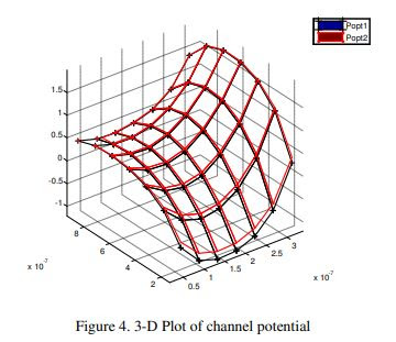
A two dimensional numerical model of an optically gated GaAs MESFET with non uniform channel doping has been developed. This is done to characterize the device as a photo detector. First photo induced voltage (Vop) at the Schottky gate is calculated for estimating the channel profile. Then Poisson’s equation for the device is solved numerically under dark and illumination condition. The paper aims at developing the MESFET 2-D model under illumination using Monte Carlo Finite Difference method. The results discuss about the optical potential developed in the device, variation of channel potential under different biasing and illumination and also about electric fields along X and Y directions. The Cgs under different illumination is also calculated. It has been observed from the results that the characteristics of the device are strongly influenced by the incident optical illumination.

KEYWORDS

Optoelectronics, Schottky Junction, Photodetectors, Photovoltage

Original Source URL: https://aircconline.com/vlsics/V1N2/0610vlsics3.pdf

https://airccse.org/journal/vlsi/vol1.html


Wednesday, 28 July 2021

Efficient Hardware Co-Simulation of Down Convertor for Wireless Communication Systems

Rajesh Mehra and Swapna Devi

Department of Electronics & Communication Engineering, Sector-26, NITTTR, Chandigarh, UT, India 

ABSTRACT

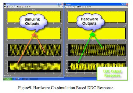
In this paper an optimized hardware co-simulation approach is presented to design & implement GSM based digital down convertor for Software Defined Radios. The proposed DDC is implemented using optimal equiripple technique to reduce the resource requirement. A computationally efficient polyphase decomposition structure is used to improve the hardware complexity of the overall design. The proposed model is implemented by using embedded multipliers, LUTs and BRAMs of target device to enhance the system performance in terms of speed and area. The DDC model is designed and simulated with Simulink and Xilinx System Generator, synthesized with Xilinx Synthesis Tool (XST) and implemented on Virtex-II Pro based xc2vp30-7ff896 FPGA device. The results show that proposed design can operate at maximum frequency of 160 MHz by consuming power of 0.34004W 25 °C junction temperature. The proposed design is consuming very less resources available on target device to provide cost effective solution for SDR based wireless applications.

KEYWORDS

ASIC, BRAM, FPGA, GSM, LUT & SDR 

Original Source URL: https://aircconline.com/vlsics/V1N2/0610vlsics2.pdf

https://airccse.org/journal/vlsi/vol1.html


Thursday, 15 July 2021

Design of Low Power Phase Locked Loop (PLL) Using 45NM VLSI Technology

Ms. Ujwala A. Belorkar 1 and Dr. S.A.Ladhake2

1Department of electronics & telecommunication ,Hanuman Vyayam Prasarak Mandal’s College of Engineering & Technology, Amravati. Maharashtra.

2Sipana’s College of Engineering & Technology, Amravati, Maharashtra.

ABSTRACT

 Power has become one of the most important paradigms of design convergence for multi gigahertz communication systems such as optical data links, wireless products, microprocessor & ASIC/SOC designs. POWER consumption has become a bottleneck in microprocessor design. The core of a microprocessor, which includes the largest power density on the microprocessor. In an effort to reduce the power consumption of the circuit, the supply voltage can be reduced leading to reduction of dynamic and static power consumption. Lowering the supply voltage, however, also reduces the performance of the circuit, which is usually unacceptable. One way to overcome this limitation, available in some application domains, is to replicate the circuit block whose supply voltage is being reduced in order to maintain the same throughput .This paper introduces a design aspects for low power phase locked loop using VLSI technology. This phase locked loop is designed using latest  45nm process technology parameters, which in turn offers high speed performance at low power. The main novelty related to the 45nm technology such as the high-k gate oxide ,metal-gate and very low-k interconnect dielectric described. VLSI Technology includes process design, trends, chip fabrication, real circuit parameters, circuit design, electrical characteristics, configuration building blocks, switching circuitry, translation onto silicon, CAD, practical experience in layout design

KEYWORDS

Phase locked loop (PLL), voltage-controlled oscillator (VCO), 45nm technology, VLSI technology, low power. 

Original Source URL: https://aircconline.com/vlsics/V1N2/0610vlsics1.pdf

https://airccse.org/journal/vlsi/vol1.html