Wednesday 28 July 2021

Efficient Hardware Co-Simulation of Down Convertor for Wireless Communication Systems

Rajesh Mehra and Swapna Devi

Department of Electronics & Communication Engineering, Sector-26, NITTTR, Chandigarh, UT, India 

ABSTRACT

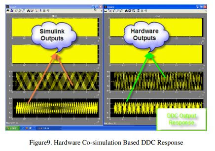
In this paper an optimized hardware co-simulation approach is presented to design & implement GSM based digital down convertor for Software Defined Radios. The proposed DDC is implemented using optimal equiripple technique to reduce the resource requirement. A computationally efficient polyphase decomposition structure is used to improve the hardware complexity of the overall design. The proposed model is implemented by using embedded multipliers, LUTs and BRAMs of target device to enhance the system performance in terms of speed and area. The DDC model is designed and simulated with Simulink and Xilinx System Generator, synthesized with Xilinx Synthesis Tool (XST) and implemented on Virtex-II Pro based xc2vp30-7ff896 FPGA device. The results show that proposed design can operate at maximum frequency of 160 MHz by consuming power of 0.34004W 25 °C junction temperature. The proposed design is consuming very less resources available on target device to provide cost effective solution for SDR based wireless applications.

KEYWORDS

ASIC, BRAM, FPGA, GSM, LUT & SDR 

Original Source URL: https://aircconline.com/vlsics/V1N2/0610vlsics2.pdf

https://airccse.org/journal/vlsi/vol1.html


Thursday 15 July 2021

Design of Low Power Phase Locked Loop (PLL) Using 45NM VLSI Technology

Ms. Ujwala A. Belorkar 1 and Dr. S.A.Ladhake2

1Department of electronics & telecommunication ,Hanuman Vyayam Prasarak Mandal’s College of Engineering & Technology, Amravati. Maharashtra.

2Sipana’s College of Engineering & Technology, Amravati, Maharashtra.

ABSTRACT

 Power has become one of the most important paradigms of design convergence for multi gigahertz communication systems such as optical data links, wireless products, microprocessor & ASIC/SOC designs. POWER consumption has become a bottleneck in microprocessor design. The core of a microprocessor, which includes the largest power density on the microprocessor. In an effort to reduce the power consumption of the circuit, the supply voltage can be reduced leading to reduction of dynamic and static power consumption. Lowering the supply voltage, however, also reduces the performance of the circuit, which is usually unacceptable. One way to overcome this limitation, available in some application domains, is to replicate the circuit block whose supply voltage is being reduced in order to maintain the same throughput .This paper introduces a design aspects for low power phase locked loop using VLSI technology. This phase locked loop is designed using latest  45nm process technology parameters, which in turn offers high speed performance at low power. The main novelty related to the 45nm technology such as the high-k gate oxide ,metal-gate and very low-k interconnect dielectric described. VLSI Technology includes process design, trends, chip fabrication, real circuit parameters, circuit design, electrical characteristics, configuration building blocks, switching circuitry, translation onto silicon, CAD, practical experience in layout design

KEYWORDS

Phase locked loop (PLL), voltage-controlled oscillator (VCO), 45nm technology, VLSI technology, low power. 

Original Source URL: https://aircconline.com/vlsics/V1N2/0610vlsics1.pdf

https://airccse.org/journal/vlsi/vol1.html


Friday 2 July 2021

Design of a High Precision, Wide Ranged Analog Clock Generator with Field Programmability Using Floating-Gate Transistors

Garima Kapur, C.M Markan and V. Prem Pyara, Dayalbagh Educational Institute, India

ABSTRACT

This paper presents a circuit of a high-precision, wide ranged, analog clock generator with on-chip programmability feature using Floating-gate transistors. The programmable oscillator can attain a continuous range of time-periods lying in the programming precision range of Floating Gates. The circuit consists of two sub circuits: Current Generator circuit and Wave Generator circuit. The current of current generator circuit is programmable and mirrored to the wave generator to generate the desired square wave. The topology is well suited to applications like clocking high performance ADCs and DACs as well as used as the internal clock in structured analog CMOS designs. A simulation model of the circuit was built in T-Spice, 0.35µm CMOS process. The circuit results in finely tuned clock with programmability precision of about 13bit [1]. Simulation results show high amount of temperature insensitivity (0.507ns/°C) for a large range of thermal conditions. The proposed circuit can compensate any change in temperature. The circuit design can be operated at low supply voltage i.e., 1v.

KEYWORDS

Square wave generator, floating gate FET, field programmability

Original Source URL: https://aircconline.com/vlsics/V1N3/0910vlsics05.pdf

http://airccse.org/journal/vlsi/vol1.html