Wednesday 24 February 2021

Design and Analysis of A 32-bit Pipelined MIPS Risc Processor

P. Indira1, M. Kamaraju2 and Ved Vyas Dwivedi3

1,3Department of Electronics and Communication Engineering, CU Shah University, Wadhwan, Gujarat, India

2Department of Electronics and Communication Engineering,Gudlavalleru Engineering College, JNT University, Kakinada, Andhra Pradesh, India

ABSTRACT

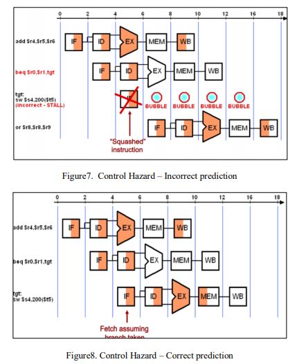
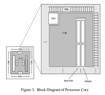
Pipelining is a technique that exploits parallelism, among the instructions in a sequential instruction stream to get increased throughput, and it lessens the total time to complete the work. . The major objective of this architecture is to design a low power high performance structure which fulfils all the requirements of the design. The critical factors like power, frequency, area, propagation delay are analysed using Spartan 3E XC3E 1600e device with Xilinx tool. In this paper, the 32-bit MIPS RISC processor is used in 6-stage pipelining to optimize the critical performance factors. The fundamental functional blocks of the processor include Input/Output blocks, configurable logic blocks, Block RAM, and Digital clock Manager and each block permits to connect to multiple sources for the routing. The Auxiliary units enhance the performance of the processor. The comparative study elevates the designed model in terms of Area, Power and Frequency. MATLAB2D/3D graphs represents the relationship among various parameters of this pipelining. In this pipeline model, it consumes very less power (0.129 W),path delay (11.180 ns) and low LUT utilization (421). Similarly, the proposed model achieves better frequency increase (285.583 Mhz.), which obtained better results compared to other models.

KEYWORDS

MATLAB, SPARTAN3E, MIPS RISC processor, Xilinx, Digital Clock Manager

Original Source URL: https://aircconline.com/vlsics/V10N5/10519vlsi01.pdf

http://airccse.org/journal/vlsi/vol10.html


Saturday 20 February 2021

Wednesday 17 February 2021

Design And Implementation of Combined Pipelining and Parallel Processing Architecture for FIR and IIR Filters Using VHDL

Jacinta Potsangbam1 and Manoj Kumar2

1M. Tech VLSI Design, Dept. of ECE, National Institute of Technology, Manipur, India

2Assistant Professor, Dept. of ECE, National Institute of Technology, Manipur, India

ABSTRACT

Along with the advancement in VLSI (Very Large Scale Integration) technology, the implementation of Finite impulse response (FIR) filters and Infinite impulse response (IIR) filters with enhanced speed has become more demanding. This paper aims at designing and implementing a combined pipelining and parallel processing architecture for FIR and IIR filter using VHDL (Very High Speed Integrated Circuit Hardware Descriptive Language) to reduce the power consumption and delay of the filter. The proposed architecture is compared with the original FIR and IIR filter respectively in terms of speed, area, and power. Also, the proposed architecture is compared with existing architectures in terms of delay. The implementation is done by using VHDL codes. FIR and IIR filters structures are implemented at 1200 KHz clock frequency. Synthesis and simulation have been accomplished on Artix-7 series FPGA, target device (xc7a200tfbg676) (speed grade -1) using VIVADO 2016.3.

KEYWORDS

DSP, FIR, FPGA, IIR, MIMO.

Original Source URL: https://aircconline.com/vlsics/V10N4/10419vlsi01.pdf

http://airccse.org/journal/vlsi/vol10.html


Monday 8 February 2021

Top 10 Cited Articles in VLSI Design & Communication Systems Research: January 2021

 International Journal of VLSI design & Communication Systems ( VLSICS ) 

ISSN: 0976 - 1357 (Online); 0976 - 1527(print)

http://airccse.org/journal/vlsi/vlsics.html

***February Issue Journal***

Top 10 Cited Articles in VLSI Design & Communication Systems Research: January 2021

https://www.academia.edu/45075723/Top_10_Cited_Articles_in_VLSI_Design_and_Communication_Systems_Research_January_2021

Submission Deadline: February 13, 2021

Contact Us

Here's where you can reach us: vlsicsjournal@airccse.org or vlsicsjournal@yahoo.com


Friday 5 February 2021

Duty Cycle Corrector Using Pulse Width Modulation

Meghana Patil1, Dr. Kiran Bailey2 and Rajanikanth Anuvanahally3

1Department of Electronics and Communication, BMSCE, Bengaluru, Karnataka, India

2Department of Electronics and Communication, BMSCE, Bengaluru, Karnataka, India

3Senior Member IEEE, Bengaluru, Karnataka, India

ABSTRACT

In circuits, clocks usually play a very important role. Whenever data needs to be sampled, it is done with respect to clock signals. It uses the edges of the clock to sample the data. So, it becomes very much necessary to see to it that the clock signals are properly received specially in receiver circuits where data sampling is done, mainly in Double data rate(DDR) circuits. Due to effects such as jitter, skew, interference, device mismatches etc., duty cycle gets affected. We come up with duty cycle correctors that ensure 50% duty cycle of the clock signals. A duty cycle corrector (DCC) with analog feedback is proposed and simulated in 45nm process technology node. The duty cycle corrector operates for MHz frequency range covering the duty cycle from 35%-65%, with +/- 1.5% accuracy. The design is simple and the power consumption is 1.01mW.

KEYWORDS

DCC, Integrator, Control voltage generator, frequency range

ORIGINAL SOURCE URL: https://aircconline.com/vlsics/V10N3/10319vlsi01.pdf

http://airccse.org/journal/vlsi/vol10.html


Wednesday 3 February 2021

9th International Conference on Signal, Image Processing and Pattern Recognition (SIPP 2021)

9th International Conference on Signal, Image Processing and Pattern Recognition (SIPP 2021)

May 29~30, 2021, Vancouver, Canada

https://ccsit2021.org/sipp/index.html

Important Dates

• Submission Deadline: February 06, 2021

• Authors Notification: February 20, 2021

• Registration & Camera-Ready Paper Due: February 28, 2021

Contact Us

Here's where you can reach us: sipp@ccsit2021.org (or) sipp_conf@yahoo.com

Submission link: https://ccsit2021.org/submission/index.php