Tuesday, 29 October 2019


International Journal of VLSI design & Communication Systems( VLSICS ) 


ISSN: 0976 - 1357 (Online); 0976 - 1527(print)

Scope & Topics 

International journal of VLSI design & Communication Systems (VLSICS) is a bi monthly open access peer-reviewed journal that publishes articles which contribute new results in all areas of VLSI Design & Communications. The goal of this journal is to bring together researchers and practitioners from academia and industry to focus on advanced VLSI Design & communication concepts and establishing new collaborations in these areas. 

Authors are solicited to contribute to this journal by submitting articles that illustrate research results, projects, surveying works and industrial experiences that describe significant advances in the VLSI design & Communications. 

Topics of interest include, but are not limited to, the following: 

* Design
* VLSI Circuits
* Computer-Aided Design (CAD)
* Low Power and Power Aware Design
* Testing, Reliability, Fault-Tolerance
* Emerging Technologies
* Post-CMOS VLSI
* VLSI Applications (Communications, Video, Security, Sensor Networks, etc)
* Nano Electronics, Molecular, Biological and Quantum Computing
* Intellectual Property Creating and Sharing
* Wireless Communications

Paper Submission 

Authors are invited to submit papers for this journal through E-mail; vlsicsjournal@airccse.org.  Submissions must be original and should not have been published previously or be under consideration for publication while being evaluated for this Journal. 

Important Dates: 

·         Submission Deadline    : November 02, 2019
·         Acceptance Notification :December 02, 2019
·         Final Manuscript Due     : December 10, 2019
·         Publication Date : Determined by the Editor-in-Chief


Friday, 25 October 2019

Most viewed article in academia

International journal of VLSI design & Communication Systems  ( VLSICS )

ISSN : 0976 - 1357  (Online); 0976 - 1527(print)


Submission Deadline          : October 26, 2019

Contact us: Here's where you can reach us:  vlsicsjournal@airccse.org 

Submission link: https://coneco2009.com/submissions/imagination/home.html

Paper Title: VERIFICATION OF DRIVER LOGIC USING AMBA- AXI UVM

Acadamia Link: https://www.academia.edu/36956674/VERIFICATION_OF_DRIVER_LOGIC_USING_AMBA-_AXI_UVM

Thursday, 24 October 2019

TOP 2 CITED PAPERS 2017 IN VLSI DESIGN @ COMMUNICATION SYSTEMS

International journal of VLSI design & Communication Systems  ( VLSICS )


ISSN : 0976 - 1357  (Online); 0976 - 1527(print)

Contact US:  vlsicsjournal@airccse.org

Please Visit the link:https://www.academia.edu/40718177/TOP_2_CITED_PAPERS_2017_IN_VLSI_DESIGN_at_COMMUNICATION_SYSTEMS

Wednesday, 23 October 2019

10th International Conference on VLSI (VLSI 2019)

December 21~22, 2019, Sydney, Australia


Contact Us:  vlsi@cndc2019.org or vlsiconfe@yahoo.com

IMPORTANT DATES

Submission Deadline : October 26, 2019
Authors Notification : November 15, 2019
Registration & Camera-Ready Paper Due : November 23, 2019

Paper Submission Url: http://cndc2019.org/submission/index.php


DESIGN OF LOW POWER MEDICAL DEVICE

Wei Cai1 and Frank Shi2

1Department of Electrical Engineering and Computer Science, University of California, Irvine, USA

2HHS School of Engineering, University of California, Irvine, USA

ABSTRACT

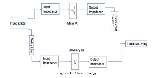
This paper describes the design of an MMIC phase shifter which can be used in a 4-channel 26-28 GHZ transmitter IC. The MMIC phase shifter is used for 5G RF front Ended applications. MMICs usually include power amplifiers with 4-bit digital phase shifters to make the phase adjustable. The whole design was used for the transmit chain of a mobile device and in a base-station.Future topology will continue to be improved.

KEYWORDS

Doherty Power Amplifier, MMIC, phase shifter


Monday, 21 October 2019

VLSICS Google Scholar Citation Graph

International Journal of VLSI design & Communication Systems (VLSICS) 

ISSN : 0976 - 1357  (Online); 0976 - 1527(print)  


VLSICS Google Scholar LINK:https://scholar.google.com/citations?user=ZdE-aVMAAAAJ&hl=en


Thursday, 17 October 2019


SURVEY ON POWER OPTIMIZATION TECHNIQUES FOR LOW POWER VLSI CIRCUIT IN DEEP SUBMICRON TECHNOLOGY

T. Suguna and M. Janaki Rani

Department of Electronics and Communication Engineering, Dr.M.G. R Educational and Research Institute, Chennai, India

ABSTRACT

CMOS technology is the key element in the development of VLSI systems since it consumes less power. Power optimization has become an overridden concern in deep submicron CMOS technologies. Due to shrink in the size of device, reduction in power consumption and over all power management on the chip are the key challenges. For many designs power optimization is important in order to reduce package cost and to extend battery life. In power optimization leakage also plays a very important role because it has significant fraction in the total power dissipation of VLSI circuits. This paper aims to elaborate the developments and advancements in the area of power optimization of CMOS circuits in deep submicron region. This survey will be useful for the designer for selecting a suitable technique depending upon the requirement.

KEYWORDS

leakage power, low power, voltage scaling, power gating, transistor stacking, adiabatic logic.