Thursday, 30 September 2021

QoS Based Capacity Enhancement for WCDMA Network with Coding Scheme

K. Ayyappan1 and R. Kumar2 

1Rajiv Gandhi College of Engineering and Technology, India and 2SRM University, India

ABSTRACT

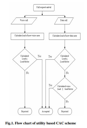
The wide-band code division multiple access (WCDMA) based 3G and beyond cellular mobile wireless networks are expected to provide a diverse range of multimedia services to mobile users with guaranteed quality of service (QoS). To serve diverse quality of service requirements of these networks it necessitates new radio resource management strategies for effective utilization of network resources with coding schemes. Call admission control (CAC) is a significant component in wireless networks to guarantee quality of service requirements and also to enhance the network resilience. In this paper capacity enhancement for WCDMA network with convolutional coding scheme is discussed and compared with block code and without coding scheme to achieve a better balance between resource utilization and quality of service provisioning. The model of this network is valid for the real-time (RT) and non-real-time (NRT) services having different data rate. Simulation results demonstrate the effectiveness of the network using convolutional code in terms of capacity enhancement and QoS of the voice and video services.

KEYWORDS

Call admission control, Wide band code division multiple access, Wireless networks, Quality of service.

Original Source URL: https://aircconline.com/vlsics/V1N1/0310vlsics2.pdf

https://airccse.org/journal/vlsi/vol1.html

#VLSIdesign #communication #AIRCC #VLSICS


Tuesday, 28 September 2021

September 2021: Top Read Articles in VLSI design & Communication Systems

 Authors are invited to submit papers!

===========================

International Journal of VLSI design & Communication Systems ( VLSICS )

ISSN: 0976 - 1357 (Online); 0976 - 1527(print)

http://airccse.org/journal/vlsi/vlsics.html

Contact Us

Here's where you can reach us : vlsicsjournal@airccse.org or vlsics@aircconline.com or vlsicsjournal@yahoo.com

Submission System: http://coneco2009.com/submissions/imagination/home.html

===========================

September 2021: Top Read Articles in VLSI design & Communication Systems

https://www.academia.edu/53655732/September_2021_Top_Read_Articles_in_VLSI_design_and_Communication_Systems


Thursday, 23 September 2021

CFP: International Journal of VLSI design & Communication Systems ( VLSICS )

 Call For Papers...!!!

=============================

International Journal of VLSI design & Communication Systems ( VLSICS )

ISSN: 0976 - 1357 (Online); 0976 - 1527(print)

http://airccse.org/journal/vlsi/vlsics.html

Contact Us

Here's where you can reach us : vlsicsjournal@airccse.org or vlsics@aircconline.com or vlsicsjournal@yahoo.com

Submission System: http://coneco2009.com/submissions/imagination/home.html

=============================

https://scholar.google.co.in/citations?user=ZdE-aVMAAAAJ


Wednesday, 15 September 2021

Design of a Low Power Low Voltage CMOS Opamp

Ratul Kr. Baruah

Department of Electronics and Communication Engineering, Tezpur University, India

ABSTRACT 

In this paper a CMOS operational amplifier is presented which operates at 2V power supply and 1uA input bias current at 0.8 um technology using non conventional mode of operation of MOS transistors and whose input is depended on bias current. The unique behaviour of the MOS transistors in subthreshold region not only allows a designer to work at low input bias current but also at low voltage. While operating the device at weak inversion results low power dissipation but dynamic range is degraded. Optimum balance between power dissipation and dynamic range results when the MOS transistors are operated at moderate inversion. Power is again minimised by the application of input dependant bias current using feedback loops in the input transistors of the differential pair with two current substractors. In comparison with the reported low power low voltage opamps at 0.8 um technology, this opamp has very low standby power consumption with a high driving capability and operates at low voltage. The opamp is fairly small (0.0084 mm2) and slew rate is more than other low power low voltage opamps reported at 0.8 um technology [1,2]. Vittoz at al [3] reported that slew rate can be improved by adaptive biasing technique and power dissipation can be reduced by operating the device in weak inversion. Though lower power dissipation is achieved the area required by the circuit is very large and speed is too small. So, operating the device in moderate inversion is a good solution. Also operating the device in subthreshold region not only allows lower power dissipation but also a lower voltage operation is achieved.

KEYWORDS

Opamp, Adaptive biasing, Low power, Low voltage, Current Substractor.

Original Source URL: https://aircconline.com/vlsics/V1N1/0310vlsics1.pdf

https://airccse.org/journal/vlsi/vol1.html